


 The Chemical Connection: Onshoring PCB Production—Daunting but Certainly Possible
 Marcy’s Musings: The Legislative Outlook—Helping or Hurting?
 It’s Only Common Sense: The Phone Is Still Mightier Than the Keyboard


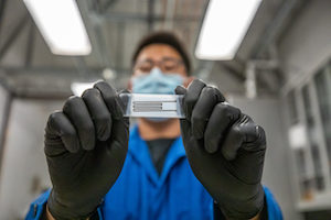
Print, Recycle, Repeat: Scientists Demonstrate a Biodegradable Printed Circuit
August 31, 2022 | Berkeley LabEstimated reading time: 4 minutes
According to the United Nations, less than a quarter of all U.S. electronic waste gets recycled. In 2021 alone, global e-waste surged at 57.4 million tons, and only 17.4% of that was recycled.
Some experts predict that our e-waste problem will only get worse over time, because most electronics on the market today are designed for portability, not recyclability. Tablets and readers, for example, are assembled by gluing circuits, chips, and hard drives to thin layers of plastic, which must be melted to extract precious metals like copper and gold. Burning plastic releases toxic gases into the atmosphere, and electronics wasting away in landfill often contain harmful materials like mercury, lead, and beryllium.
But now, a team of researchers from the Department of Energy’s Lawrence Berkeley National Laboratory (Berkeley Lab) and UC Berkeley have developed a potential solution: a fully recyclable and biodegradable printed circuit. The researchers, who reported the new device in the journal Advanced Materials, say that the advance could divert wearable devices and other flexible electronics from landfill, and mitigate the health and environmental hazards posed by heavy metal waste.
“When it comes to plastic e-waste, it’s easy to say it’s impossible to solve and walk away,” said senior author Ting Xu, a faculty senior scientist in Berkeley Lab’s Materials Sciences Division, and professor of chemistry and materials science and engineering at UC Berkeley. “But scientists are finding more evidence of significant health and environmental concerns caused by e-waste leaching into the soil and groundwater. With this study, we’re showing that even though you can’t solve the whole problem yet, you can at least tackle the problem of recovering heavy metals without polluting the environment.”
Putting enzymes to work
In a previous study, Xu and her team demonstrated a biodegradable plastic material embedded with purified enzymes such as Burkholderia cepacian lipase (BC-lipase). Through that work, they discovered that hot water activates BC-lipase, prompting the enzyme to degrade polymer chains into monomer building blocks. They also learned that BC-lipase is a finicky “eater.” Before a lipase can convert a polymer chain into monomers, it must first catch the end of a polymer chain. By controlling when the lipase finds the chain end, it is possible to ensure the materials don’t degrade until the water reaches a certain temperature.
For the current study, Xu and her team simplified the process even further. Instead of expensive purified enzymes, the biodegradable printed circuits rely on cheaper, shelf-ready BC lipase “cocktails.” This significantly reduces costs, facilitating the printed circuit’s entry into mass manufacturing, Xu said.
By doing so, the researchers advanced the technology, enabling them to develop a printable “conductive ink” composed of biodegradable polyester binders, conductive fillers such as silver flakes or carbon black, and commercially available enzyme cocktails. The ink gets its electrical conductivity from the silver or carbon black particles, and the biodegradable polyester binders act as a glue.
The researchers supplied a commercial 3D printer with the conductive ink to print circuit patterns onto various surfaces such as hard biodegradable plastic, flexible biodegradable plastic, and cloth. This proved that the ink adheres to a variety of materials, and forms an integrated device once the ink dries.
To test its shelf life and durability, the researchers stored a printed circuit in a laboratory drawer without controlled humidity or temperature for seven months. After pulling the circuit from storage, the researchers applied continuous electrical voltage to the device for a month and found that the circuit conducted electricity just as well as it did before storage.
Next, the researchers put the device’s recyclability to test by immersing it in warm water. Within 72 hours, the circuit materials degraded into its constituent parts. The silver particles completely separated from the polymer binders, and the polymers broke down into reusable monomers, allowing the researchers to easily recover the metals without additional processing. By the end of this experiment, they determined that approximately 94% of the silver particles can be recycled and reused with similar device performance.
That the circuit’s degradability continued after 30 days of operation surprised the researchers, suggesting that the enzymes were still active. “We were surprised that the enzymes ‘lived’ for so long. Enzymes aren’t designed to work in an electric field,” Xu said.
Xu attributes the working enzymes’ longevity to the biodegradable plastic’s molecular structure. In their previous study, the researchers learned that adding an enzyme protectant called random heteropolymer, or RHP, helps to disperse the enzymes within the mixture in clusters a few nanometers (billionths of a meter) in size. This creates a safe place in the plastic for enzymes to lie dormant until they’re called to action.
The circuit also shows promise as a sustainable alternative to single-use plastics used in transient electronics – devices such as biomedical implants or environmental sensors that disintegrate over a period of time, said lead author Junpyo Kwon, a Ph.D. student researcher from the Xu Group at UC Berkeley.
Now that they’ve demonstrated a biodegradable and recyclable printed circuit, Xu wants to demonstrate a printable, recyclable, and biodegradable microchip.
“Given how sophisticated chips are nowadays, this certainly won’t be easy. But we have to try and give our level best,” she said.
This work was supported by the DOE Office of Science. Additional funding was provided by the U.S. Department of Defense, Army Research Office.
The technology is available for licensing through UC Berkeley’s Office of Technology Licensing.
Share on:


Testimonial
"We’re proud to call I-Connect007 a trusted partner. Their innovative approach and industry insight made our podcast collaboration a success by connecting us with the right audience and delivering real results."
Julia McCaffrey - NCAB GroupSuggested Items
Episode 6 of Ultra HDI Podcast Series Explores Copper-filled Microvias in Advanced PCB Design and Fabrication
10/15/2025 | I-Connect007I-Connect007 has released Episode 6 of its acclaimed On the Line with... American Standard Circuits: Ultra High Density Interconnect (UHDI) podcast series. In this episode, “Copper Filling of Vias,” host Nolan Johnson once again welcomes John Johnson, Director of Quality and Advanced Technology at American Standard Circuits, for a deep dive into the pros and cons of copper plating microvias—from both the fabricator’s and designer’s perspectives.
Nolan’s Notes: Tariffs, Technologies, and Optimization
10/01/2025 | Nolan Johnson -- Column: Nolan's NotesLast month, SMT007 Magazine spotlighted India, and boy, did we pick a good time to do so. Tariff and trade news involving India was breaking like a storm surge. The U.S. tariffs shifted India from one of the most favorable trade agreements to the least favorable. Electronics continue to be exempt for the time being, but lest you think that we’re free and clear because we manufacture electronics, steel and aluminum are specifically called out at the 50% tariff levels.
MacDermid Alpha & Graphic PLC Lead UK’s First Horizontal Electroless Copper Installation
09/30/2025 | MacDermid Alpha & Graphic PLCMacDermid Alpha Electronics Solutions, a leading supplier of integrated materials and chemistries to the electronics industry, is proud to support Graphic PLC, a Somacis company, with the installation of the first horizontal electroless copper metallization process in the UK.
Electrodeposited Copper Foils Market to Grow by $11.7 Billion Over 2025-2032
09/18/2025 | Globe NewswireThe global electrodeposited copper foils market is poised for dynamic growth, driven by the rising adoption in advanced electronics and renewable energy storage solutions.
MacDermid Alpha Showcases Advanced Interconnect Solutions at PCIM Asia 2025
09/18/2025 | MacDermid Alpha Electronics SolutionsMacDermid Alpha Electronic Solutions, a global leader in materials for power electronics and semiconductor assembly, will showcase its latest interconnect innovations in electronic interconnect materials at PCIM Asia 2025, held from September 24 to 26 at the Shanghai New International Expo Centre, Booth N5-E30