


 It’s Only Common Sense: Trust Is All You Need
 Dan’s Biz Bookshelf: ‘The Future of Sales'
 Driving Innovation: Traceability in PCB Production


Cadence Introduces Industry’s Leading-Performance, Silicon-Proven 22Gbps GDDR6 IP at TSMC N5
November 16, 2022 | Cadence Design Systems, Inc.Estimated reading time: 1 minute
Cadence Design Systems, Inc. announced that Cadence IP for GDDR6 is silicon proven on TSMC’s N5 process technology, exceeding Cadence’s previous 16Gbps designs. Targeted for very high-bandwidth memory applications, including hyperscale computing, 5G communications, automotive and consumer, the GDDR6 IP consists of Cadence PHY and controller design IP and Verification IP (VIP). GDDR6 is particularly well suited for the memory interface in artificial intelligence/machine learning (AI/ML) chips, which are proliferating due to the growing number of AI inferencing applications. Customers can speed development and reduce risk when using Cadence and TSMC technologies to design these chips that connect to GDDR6 memory.
The Cadence IP for GDDR6 at TSMC N5 operating at 22Gbps offers more than 2X the data rate of other latest generation standards like DDR5 and LPDDR5 and is 37% faster than Cadence’s previous 16Gbps designs. An improved architecture allows up to 22Gbit/sec bandwidth per pin—704Gbit/sec per chip—across the full range of operating conditions, with low operational power and idle power as well as a low bit-error rate (BER) for higher reliability and greater bandwidth. The corresponding GDDR6 controller IP offers a variety of performance and reliability features derived from Cadence’s DDR controller designs.
“Cadence’s latest GDDR6 IP on TSMC’s N5 process technology has achieved a significant performance boost in silicon compared with Cadence’s previous solutions in TSMC N7, N6 and 12nm FinFET Compact (12FFC) processes,” said Dan Kochpatcharin, Head of Design Infrastructure Management Division at TSMC. “This result of our latest collaboration combining Cadence’s leading IP solutions with TSMC’s advanced process technology enables new chips in AI/ML, hyperscale, and other computationally intense applications.”
“Cadence is committed to expanding our IP portfolio to address our customers’ evolving design requirements. Customers can now capitalize on the higher bandwidth offered by the Cadence Design IP for GDDR6 on TSMC’s N5 process technology with the utmost confidence,” said Sanjive Agarwala, corporate vice president and general manager of the IP Group at Cadence. “The improved PHY and controller design IP for GDDR6 with DRAM data rates at 22Gbps in the TSMC N5 process is the fastest of the GDDR6 family of IP in advanced TSMC nodes.”
Share on:


Suggested Items
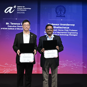
IIT Kharagpur, A*STAR Singapore Forge Strategic Partnership to Advance Semiconductor Innovation in Asia
06/03/2025 | IIT KharagpurIn a landmark move to foster global collaboration in semiconductor research and talent development, IIT Kharagpur has signed a Memorandum of Understanding (MoU) with the Institute of Microelectronics (IME) under Singapore’s Agency for Science, Technology and Research (A*STAR).
STARTEAM GLOBAL Unveils Innovative Additive Solder Mask Process
06/02/2025 | STARTEAM GLOBALSTARTEAM GLOBAL, a leading PCB manufacturer, has introduced a revolutionary additive solder mask process at its Flero STARTEAM (FST) factory in Italy, leveraging digital inkjet technology to enhance production efficiency and sustainability.
Strategic Materials Conference 2025 Spotlights Materials Innovation to Advance Semiconductor Manufacturing
06/02/2025 | SEMIWith materials innovation at the core of next-generation semiconductor technologies, the Strategic Materials Conference (SMC) 2025 brings together top executives and technology leaders from the semiconductor manufacturing industry for exclusive insights into the latest trends and advancements.
CACI to Deliver Additional SIGINT and EW Technology for U.S. Army Soldiers with TLS BCT Manpack
06/02/2025 | CACI International Inc.CACI International Inc announced that a contract modification has been awarded by the U.S. Army to continue procurement, training, and fielding for the Terrestrial Layer System Brigade Combat Team Manpack (TLS BCT Manpack).
Hon Hai Research Institute Partners with Taiwan Academic Research Institute and KAUST to Participate in CLEO 2025
05/30/2025 | FoxconnThe research team of the Semiconductor Division of Hon Hai Research Institute, together with the research teams of National Taiwan University and King Abdullah University of Science and Technology in Saudi Arabia, has successfully made breakthroughs in multi-wavelength μ -LED technology to achieve high-speed visible light communication and optical interconnection between chips.