


 The Chemical Connection: Onshoring PCB Production—Daunting but Certainly Possible
 It’s Only Common Sense: The Phone Is Still Mightier Than the Keyboard


Imec’s Nanomesh Electrodes in Pole Position for High-throughput Electrochemical Applications
December 28, 2022 | ImecEstimated reading time: 2 minutes
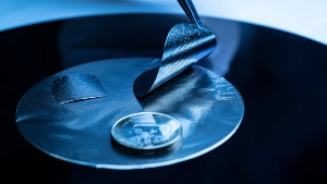
Imec, together with its partner KU Leuven in EnergyVille, announces an important proof point towards implementation of nanomesh structures in high-throughput industrial processes for energy-related applications such as electrolysers, fuel cells and batteries. The researchers have developed a 3D structure made of interconnected nanowires, which can now be used as a freestanding electrode in electrochemical flow cells. The results, published in Materials Today Energy, confirm that the use of these structures can yield a 100-fold increase in current density compared to conventional planar nickel electrodes.
Large-scale production of green hydrogen and green hydrocarbons becomes essential to decarbonize industries. Today, two commercially available options exist for megawatt-scale hydrogen production: classical alkaline water electrolysis (AWE) and proton exchange membrane electrolysis (PEM). However, both technologies face challenges that need to be overcome to further improve the competitiveness of large-scale production of green hydrogen.
Researchers from imec and KU Leuven developed a 3D structure of interconnected nanowires. These nanomesh structures combine high porosity with an extremely high surface area, providing plenty of reaction sites. Due to its unique material properties, nanomesh structures are attractive for numerous electrochemical applications, including electrolysis. They can be created via electroplating, an up-scalable fabrication flow, which makes them cheaper than currently used metal foams.
Until now, non-porous support substrates were needed to provide sufficient mechanical robustness to the highly porous nanomesh. However, to exploit these compelling nano-architectures as freestanding electrodes in electrochemical flow cells, it is essential that the gaseous reagents and products can freely flow in and out. Therefore, the nanowire networks must be supported by a porous structure that is accessible from all sides.
Researchers from imec now published their results on a monolithically integrated nickel nanomesh with an open support grid. This improved nanomesh structure allows gaseous reagents and products to be introduced and removed efficiently from the reaction sites. In an experimental setup they demonstrated that the theoretically available surface area of the nanomesh is almost completely available; resulting in a 100-fold current density increase compared to using conventional planar nickel electrodes. The results confirm that the 3.5 micrometer thin nanomesh electrode has incredible potential in throughput and conversion rates.
"To achieve large-scale production of green hydrogen at offshore wind farms, where space is limited, we need to develop compact electrolysers with high efficiency," said Bart Onsia, business development manager at imec. "These results are a promising step towards the development of new electrolysers components, and we are committed to continuing our research in this area to drive the transition to a more sustainable future."
Philippe Vereecken, imec fellow and part-time professor at KU Leuven: “I am excited that we have been able to further enhance our nanomesh materials and demonstrate their potential in an industry-relevant setup. We have chosen nickel for the current demonstrations for hydrogen production, an area in which we partner with VITO within Hyve, a Belgian consortium that pursues cost-efficient and sustainable hydrogen production on gigawatt scale."
“And the versatility of the nanomesh allows for a much wider portfolio of materials and applications. For instance, we can use copper or silver for CO2 reduction in gas diffusion electrodes," adds Nina Planckensteiner, Marie-Curie post-doctoral researcher at imec. “We are excited to continue exploring the potential of the nanomesh for a wide range of electrochemical applications.”
Share on:


Testimonial
"Advertising in PCB007 Magazine has been a great way to showcase our bare board testers to the right audience. The I-Connect007 team makes the process smooth and professional. We’re proud to be featured in such a trusted publication."
Klaus Koziol - atgSuggested Items
Episode 6 of Ultra HDI Podcast Series Explores Copper-filled Microvias in Advanced PCB Design and Fabrication
10/15/2025 | I-Connect007I-Connect007 has released Episode 6 of its acclaimed On the Line with... American Standard Circuits: Ultra High Density Interconnect (UHDI) podcast series. In this episode, “Copper Filling of Vias,” host Nolan Johnson once again welcomes John Johnson, Director of Quality and Advanced Technology at American Standard Circuits, for a deep dive into the pros and cons of copper plating microvias—from both the fabricator’s and designer’s perspectives.
Nolan’s Notes: Tariffs, Technologies, and Optimization
10/01/2025 | Nolan Johnson -- Column: Nolan's NotesLast month, SMT007 Magazine spotlighted India, and boy, did we pick a good time to do so. Tariff and trade news involving India was breaking like a storm surge. The U.S. tariffs shifted India from one of the most favorable trade agreements to the least favorable. Electronics continue to be exempt for the time being, but lest you think that we’re free and clear because we manufacture electronics, steel and aluminum are specifically called out at the 50% tariff levels.
MacDermid Alpha & Graphic PLC Lead UK’s First Horizontal Electroless Copper Installation
09/30/2025 | MacDermid Alpha & Graphic PLCMacDermid Alpha Electronics Solutions, a leading supplier of integrated materials and chemistries to the electronics industry, is proud to support Graphic PLC, a Somacis company, with the installation of the first horizontal electroless copper metallization process in the UK.
Electrodeposited Copper Foils Market to Grow by $11.7 Billion Over 2025-2032
09/18/2025 | Globe NewswireThe global electrodeposited copper foils market is poised for dynamic growth, driven by the rising adoption in advanced electronics and renewable energy storage solutions.
MacDermid Alpha Showcases Advanced Interconnect Solutions at PCIM Asia 2025
09/18/2025 | MacDermid Alpha Electronics SolutionsMacDermid Alpha Electronic Solutions, a global leader in materials for power electronics and semiconductor assembly, will showcase its latest interconnect innovations in electronic interconnect materials at PCIM Asia 2025, held from September 24 to 26 at the Shanghai New International Expo Centre, Booth N5-E30