


 Dan’s Biz Bookshelf: ‘Do/Start'
 Facing the Future: The Role of 5G and Beyond in Shaping PCB Demand
 It’s Only Common Sense: Stop Pitching, Start Listening


3D-printed Antenna
March 17, 2016 | ESAEstimated reading time: 1 minute
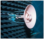
A prototype 3D-printed antenna being put to work in ESA’s Compact Antenna Test Facility, a shielded chamber for antenna and radio-frequency testing.
“This is the Agency’s first 3D-printed dual-reflector antenna,” explains engineer Maarten van der Vorst, who designed it.
“Incorporating a corrugated feedhorn and two reflectors, it has been printed all-in-one in a polymer, then plated with copper to meet its radio-frequency (RF) performance requirements.
“Designed for future mega-constellation small satellite platforms, it would need further qualification to make it suitable for real space missions, but at this stage we’re most interested in the consequences on RF performance of the low-cost 3D-printing process.”
“Although the surface finish is rougher than for a traditionally manufactured antenna, we’re very happy with the resulting performance,” says antenna test engineer Luis Rolo.
“We have a very good agreement between the measurements and the simulations. Making a simulation based on a complete 3D model of the antenna leads to a significant increase in its accuracy.
“By using this same model to 3D print it in a single piece, any source of assembly misalignments and errors are removed, enabling such excellent results.”
Two different antennas were produced by Swiss company SWISSto12, employing a special copper-plating technique to coat the complex shapes.
“As a next step, we aim at more complex geometries and target higher frequencies,” adds Maarten, a member of ESA’s Electromagnetics & Space Environment Division. “And eventually we want to build space-qualified RF components for Earth observation and science instruments.”
Based at ESA’s ESTEC technical centre in Noordwijk, the Netherlands, the test range is isolated from outside electromagnetic radiation while its inside walls are covered with ‘anechoic’ foam to absorb radio signals, simulating infinite space.
The range is part of ESA’s suite of antenna testing facilities, intended for smaller antennas and subsystems, with larger antennas and entire satellites put to the test in its ‘big brother’, the Hertz chamber.
Share on:


Suggested Items
RF PCB Design Tips and Tricks
05/08/2025 | Cherie Litson, EPTAC MIT CID/CID+There are many great books, videos, and information online about designing PCBs for RF circuits. A few of my favorite RF sources are Hans Rosenberg, Stephen Chavez, and Rick Hartley, but there are many more. These PCB design engineers have a very good perspective on what it takes to take an RF design from schematic concept to PCB layout.
Trouble in Your Tank: Causes of Plating Voids, Pre-electroless Copper
05/09/2025 | Michael Carano -- Column: Trouble in Your TankIn the business of printed circuit fabrication, yield-reducing and costly defects can easily catch even the most seasoned engineers and production personnel off guard. In this month’s column, I’ll investigate copper plating voids with their genesis in the pre-plating process steps.
Elephantech: For a Greener Tomorrow
04/16/2025 | Marcy LaRont, PCB007 MagazineNobuhiko Okamoto is the global sales and marketing manager for Elephantech Inc., a Japanese startup with a vision to make electronics more sustainable. The company is developing a metal inkjet technology that can print directly on the substrate and then give it a copper thickness by plating. In this interview, he discusses this novel technology's environmental advantages, as well as its potential benefits for the PCB manufacturing and semiconductor packaging segments.
Trouble in Your Tank: Organic Addition Agents in Electrolytic Copper Plating
04/15/2025 | Michael Carano -- Column: Trouble in Your TankThere are numerous factors at play in the science of electroplating or, as most often called, electrolytic plating. One critical element is the use of organic addition agents and their role in copper plating. The function and use of these chemical compounds will be explored in more detail.
IDTechEx Highlights Recyclable Materials for PCBs
04/10/2025 | IDTechExConventional printed circuit board (PCB) manufacturing is wasteful, harmful to the environment and energy intensive. This can be mitigated by the implementation of new recyclable materials and technologies, which have the potential to revolutionize electronics manufacturing.