


 The Marketing Minute: Marketing With Layers
 The Right Approach: Electro-Tek—A Williams Family Legacy, Part 1
 It’s Only Common Sense: If You’re Not Differentiated, You’re Dead


MechSE Researchers Create One-step Graphene Patterning Method
April 28, 2016 | University of IllinoisEstimated reading time: 2 minutes
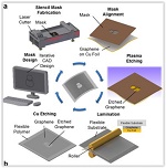
Researchers from the University of Illinois at Urbana-Champaign have developed a one-step, facile method to pattern graphene by using stencil mask and oxygen plasma reactive-ion etching, and subsequent polymer-free direct transfer to flexible substrates.
Graphene, a two-dimensional carbon allotrope, has received immense scientific and technological interest. Combining exceptional mechanical properties, superior carrier mobility, high thermal conductivity, hydrophobicity, and potentially low manufacturing cost, graphene provides a superior base material for next generation bioelectrical, electromechanical, optoelectronic, and thermal management applications.
“Significant progress has been made in the direct synthesis of large-area, uniform, high quality graphene films using chemical vapor deposition (CVD) with various precursors and catalyst substrates,” explained SungWoo Nam, an assistant professor of mechanical science and engineeringat Illinois. “However, to date, the infrastructure requirements on post-synthesis processing—patterning and transfer—for creating interconnects, transistor channels, or device terminals have slowed the implementation of graphene in a wider range of applications.”“In conjunction with the recent evolution of additive and subtractive manufacturing techniques such as 3D printing and computer numerical control milling, we developed a simple and scalable graphene patterning technique using a stencil mask fabricated via a laser cutter,” stated Keong Yong, a graduate student and first author of the paper, “Rapid Stencil Mask Fabrication Enabled One-Step Polymer-Free Graphene Patterning and Direct Transfer for Flexible Graphene Devices" appearing in Scientific Reports.
“Our approach to patterning graphene is based on a shadow mask technique that has been employed for contact metal deposition,” Yong added. “Not only are these stencil masks easily and rapidly manufactured for iterative rapid prototyping, they are also reusable, enabling cost-effective pattern replication. And since our approach involves neither a polymeric transfer layer nor organic solvents, we are able to obtain contamination-free graphene patterns directly on various flexible substrates.”Nam stated that this approach demonstrates a new possibility to overcome limitations imposed by existing post-synthesis processes to achieve graphene micro-patterning. Yong envisions this facile approach to graphene patterning sets forth transformative changes in “do It yourself” (DIY) graphene-based device development for broad applications including flexible circuits/devices and wearable electronics.
“This method allows rapid design iterations and pattern replications, and the polymer-free patterning technique promotes graphene of cleaner quality than other fabrication techniques,” Nam said. “We have shown that graphene can be patterned into varying geometrical shapes and sizes, and we have explored various substrates for the direct transfer of the patterned graphene.”
In addition to Nam and Yong, study co-authors include Ali Ashraf and Pilgyu Kang from the Department of Mechanical Science and Engineering at Illinois.
Share on:


Testimonial
"Your magazines are a great platform for people to exchange knowledge. Thank you for the work that you do."
Simon Khesin - Schmoll MaschinenSuggested Items
Elephantech's SustainaCircuits FPC Adopted for Mass Production in OM Digital Solutions’ Interchangeable Lens
10/06/2025 | ElephantechElephantech Inc. is pleased to announce that its proprietary flexible printed circuits (FPCs) have been adopted for mass production by OM Digital Solutions Corporation in the company’s latest flagship products.
Industry Expert, Mark Finstad From Flexible Circuit Technologies Presents Ask the Flexperts at PCB West
09/22/2025 | Flexible Circuit TechnologiesFlexible Circuit Technologies., Inc/FCT is excited to announce its upcoming session, Ask the Flexperts taking place Thursday, October 2nd, from 9:00–11:00 AM at PCB West 2025. The session will be led by Mark Finstad, Director or Applications Engineering at FCT, who brings over 40 years of experience in the design, fabrication, and testing of flexible and rigid-flex circuits. Mark is an internationally recognized authority in the field, making this a must-attend event for PCB designers, engineers, and industry professionals.
Printed Electronics Market Size to Top $83.77 Billion by 2034 Driven by IoT Adoption and Flexible Device Demand
09/11/2025 | Globe NewswireThe printed electronics market size has been calculated at U$19,920 million in 2025 and is expected to grow from $23,58 million in 2026 to approximately $83,770 million by 2034.
Fresh PCB Concepts: Designing for Success at the Rigid-flex Transition Area
08/28/2025 | Team NCAB -- Column: Fresh PCB ConceptsRigid-flex PCBs come in all shapes and sizes. Manufacturers typically use fire-retardant, grade 4 (FR-4) materials in the rigid section and flexible polyimide materials in the flex region. Because of the small size, some rigid-flex PCBs, like those for hearing aid devices, are among the most challenging to manufacture. However, regardless of its size, we should not neglect the transition area between the rigid and flexible material.
Global Flexible PCB Output Expected to Surpass $20 Billion by 2025, with AI Glasses Emerging as a New Growth Driver
08/25/2025 | TPCAThe Taiwan Printed Circuit Association (TPCA) and the Industrial Technology Research Institute (ITRI) released the "2025 Global Flexible PCB Industry Outlook" in August.