


 Dan’s Biz Bookshelf: ‘Abundance: How We Build a Better Future’
 Trouble in Your Tank: In Complex Systems, Design Rules Aren’t Optional
 It’s Only Common Sense: The Phone Is Still Your Competitive Advantage


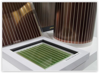
Hybrid Solar Cells Have Applications in Flexible Electronics and Portable Devices
August 15, 2016 | KAUSTEstimated reading time: 2 minutes
Understanding the impact of surface defects underpins the improved efficiency of hybrid organic/inorganic solar cells.
Hybrid solar cells utilize an interface comprising layers of organic and inorganic materials to convert sunlight into electricity. Zinc oxide (ZnO) is a popular choice for the inorganic material because it is cheap, non-toxic and readily available. However, the conversion efficiency of hybrid solar cells using ZnO/organic-donor bulk heterojunctions is currently very low—only 2 percent when ZnO is blended into an organic donor material. On the other hand, a decent 6.1 percent efficiency has been reached when ZnO is used as a layer sandwiched between an electrode and a layer of polymer or small-molecule acceptors.
Jean-Luc Bredas from the KAUST Solar & Photovoltaics Engineering Research Center and colleague Hong Li suspect that intrinsic defects in ZnO are a key factor in the poor performance1. By comparing the differences in electronic properties between various hybrid materials, they concluded that zinc vacancies reduce conversion efficiency by hindering the charge separation process at the interface between the organic and inorganic materials.
It is well known that ZnO adopts different roles in bulk heterojunctions depending on the type of organic material and architecture used. When blended with polymer or small-molecular donors such as sexithienyl, ZnO assumes the role of an electron acceptor: it takes up or "accepts" electrons and leaves positively charged holes behind in a sexithienyl layer.
When sandwiched between an electrode and a fullerene acceptor layer, ZnO helps transfer the electrons from the fullerene layer to the electrode. These processes enable the efficient conversion of sunlight into electricity.
The researchers used computer simulations to examine how zinc vacancies at the surface of zinc oxide impact these two processes. For the ZnO/sexithienyl bulk heterojunction, zinc vacancies at the ZnO surface can hinder local charge transfer at the ZnO/sexithienyl interface and can also prevent efficient charge separation due to strong Coulomb interactions. However, for the ZnO/fullerene interface, such vacancies don’t significantly impact the charge transfer process.
For these reasons, the ZnO/organic heterojunctions developed so far are inefficient. In comparison, however, zinc vacancies have significantly higher negative impact on ZnO/sexithienyl than on ZnO/fullerene interfaces. The results have important implications for the development of hybrid solar cells, which have applications in flexible electronics and portable devices.
“What we learned from our investigations is to what extent defects at the surface of conducting metal oxides like ZnO determine the overall electronic properties and ultimately the device efficiencies,” noted Bredas. He suggested the findings indicate possible ways to improve solar cell efficiency through surface modifications.
Share on:


Subscribe
Stay ahead of the technologies shaping the future of electronics with our latest newsletter, Advanced Electronics Packaging Digest. Get expert insights on advanced packaging, materials, and system-level innovation, delivered straight to your inbox.
Subscribe now to stay informed, competitive, and connected.
Suggested Items
Connect the Dots: Designing for the Future of Manufacturing Reality—Surface Finish
05/07/2026 | Matt Stevenson -- Column: Connect the DotsWhen designing the complex boards that many electronic devices require to operate, designers should consider manufacturability at every step. This is my last article focused on designing for the always-evolving manufacturing reality. Choosing the right surface finish has always been important. If you are creating intricate designs with a wide variety of components, like for an ultra-high density interconnect (UHDI) board, surface finish is a critical last step.
Elsyca Acquires Hivelix to Strengthen Simulation Platform for Electrochemical Surface Engineering
04/03/2026 | ElsycaElsyca, a global pioneer in computer-aided engineering (CAE) simulation for electrochemical processes and surface finishing, announces the acquisition of Hivelix, a specialist in advanced surface treatment simulation with strong expertise in multiphysics modelling and AI-assisted process optimisation.
Connect the Dots: Designing for the Future of Manufacturing Reality—Solder Mask and Legend
04/09/2026 | Matt Stevenson -- Column: Connect the DotsPCBs seem to be getting more complex by the day, so it is important for designers to keep educating themselves about the realities of manufacturing increasingly intricate boards. Last month’s column highlighted design considerations for the strip-etch-strip process and how manufacturers approach that phase of production. Now that we have a functioning board, we must protect the PCB from environmental hazards and document the circuit components. This article will detail the solder mask and legend process and offer best practices for designers to ensure a high-quality result.
Take the Mic: Photo Chemical Systems: 50 Years Strong
04/03/2026 | Real Time with... APEX EXPOPhoto Chemical Systems is celebrating 50 years in the bare board PCB market. David Graves and Jason Averette discuss how they've expanded into assembly, leveraging strong relationships and a customer-centric approach to navigate supply chain challenges. With innovative solutions and future growth strategies, including AI integration and new market ventures, Photo Chemical Systems continues enduring success.
Bold Laser Automation Introduces Precision Laser Cleaning System for Advanced Manufacturing
03/27/2026 | PRNewswireBold Laser Automation, Inc. has introduced the LPCl1820UV Laser Precision Cleaning System, a Class 1, industrial laser platform engineered for high-precision surface cleaning and thin-film removal in demanding manufacturing environments.