


 Trouble in Your Tank: Implementing Direct Metallization in Advanced Substrate Packaging
 It’s Only Common Sense: Storytelling That Sells—Stop Pitching, Start Painting Pictures
 The Right Approach: Get Ready for ISO 9001 Version 6


Copper Laminates Made From Transparent Polyimide Films Now Available
August 26, 2016 | DKN ResearchEstimated reading time: 3 minutes
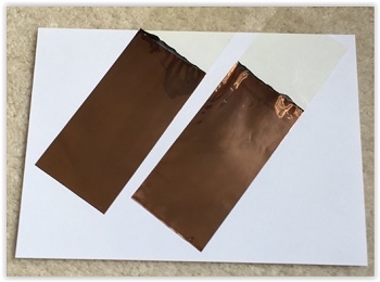
Significant progress has been made over the last few years in building transparent and heat resistant flexible circuits. Several transparent materials were developed along with special manufacturing processes. A copper laminate made from a thin transparent polyimide file plated with a copper layer on both sides for use in traditional manufacturing processes is now available. DKN Research developed a new copper metalizing process using transparent polyimide films. The new laminate will provide manufacturing capabilities using transparent flexible circuits for traditional printed circuit manufacturers.
Polyimide films are the primary substrate material for heat resistant flexible circuits because of the balanced performances between heat resistance and physical properties. The problem is they tend to have an orange or brown color, so the film’s transparency is very low. This is a huge barrier for any optical applications. PET films are another popular substrate material for transparent flexible circuits, but their heat resistance is too low and will not work in standard assembling processes such as soldering and wire bonding. A couple of new heat resistant resins such as LCP have been synthesized and are considered the next generation material for flexible circuits; however, they may not be transparent either. Many chemists used to question the availability of a product that is both transparent and heat resistant. That has changed. Several chemists were successful in synthesizing transparent polyimide resins, and a few companies have brought to market some thin transparent polyimide films that serve as the substrate for heat-resistant flexible circuits.
There are still a few technical hurdles in building transparent flexible circuits. The biggest one is the availability of an appropriate copper laminate for the standard photolithography/chemical etching process. Some of the copper laminates had problems with the surface treatment and gluing of the copper. The transparency of the circuits was remarkably reduced by absorption and scattering.
DKN Research developed a total solutions package for transparent flexible circuits based on each application. During the R&D process, DKN Research has established an electroless and electroplating process of nickel, copper and gold on the transparent polyimide films that provides thin copper laminates available for the standard photolithography/etching process of high density flexible circuits. The new copper laminate could be valuable for traditional flexible circuit manufacturers, because the new laminate does not need any additional equipment or chemicals to build transparent flexible circuits. The transparency of the circuits can be over 85%.
The standard construction of the laminate uses double-sided 3-micron thick copper layers on a 25-micron thick transparent polyimide film. The copper thickness can be thinner at 0.2 microns, and wider thickness ranges will be available for circuit manufacturers. The thin copper conductor could be valuable for semi-additive processes for ultra-fine flexible circuits with microvia holes in the transparent flexible circuits. DKN Research will provide free laminate samples along with a processing guide to circuit manufacturers.
DKN Research will upgrade the laminates and process capabilities to build the leading edge flexible circuits. DKN Research is happy to share the materials and information with circuit manufacturers and device manufacturers. Click here to view a short clip about their products and services.
About DKN Research
DKN Research is a global engineering leader for microelectronics and packaging, specializing in printable & flexible electronics. DKN Research has developed a broad range of leading edge technologies from materials to final devices based on customers’ requirements. They are capable of managing many kinds of materials and manufacturing processes to build and create new devices based on customer needs.
DKN Research provides a broad range of engineering and consulting services not only for the manufacturing community but also the R&D and quality assurance professionals. DKN Research welcomes all inquiries to assist in creating your own circuit devices using its broad range of processing technologies.
Share on:


Testimonial
"In a year when every marketing dollar mattered, I chose to keep I-Connect007 in our 2025 plan. Their commitment to high-quality, insightful content aligns with Koh Young’s values and helps readers navigate a changing industry. "
Brent Fischthal - Koh YoungSuggested Items
Trouble in Your Tank: Implementing Direct Metallization in Advanced Substrate Packaging
09/15/2025 | Michael Carano -- Column: Trouble in Your TankDirect metallization systems based on conductive graphite are gaining popularity throughout the world. The environmental and productivity gains achievable with this process are outstanding. Direct metallization reduces the costs of compliance, waste treatment, and legal issues related to chemical exposure. A graphite-based direct plate system has been devised to address these needs.
Closing the Loop on PCB Etching Waste
09/09/2025 | Shawn Stone, IECAs the PCB industry continues its push toward greener, more cost-efficient operations, Sigma Engineering’s Mecer System offers a comprehensive solution to two of the industry’s most persistent pain points: etchant consumption and rinse water waste. Designed as a modular, fully automated platform, the Mecer System regenerates spent copper etchants—both alkaline and acidic—and simultaneously recycles rinse water, transforming a traditionally linear chemical process into a closed-loop system.
Driving Innovation: Depth Routing Processes—Achieving Unparalleled Precision in Complex PCBs
09/08/2025 | Kurt Palmer -- Column: Driving InnovationIn PCB manufacturing, the demand for increasingly complex and miniaturized designs continually pushes the boundaries of traditional fabrication methods, including depth routing. Success in these applications demands not only on robust machinery but also sophisticated control functions. PCB manufacturers rely on advanced machine features and process methodologies to meet their precise depth routing goals. Here, I’ll explore some crucial functions that empower manufacturers to master complex depth routing challenges.
Trouble in Your Tank: Minimizing Small-via Defects for High-reliability PCBs
08/27/2025 | Michael Carano -- Column: Trouble in Your TankTo quote the comedian Stephen Wright, “If at first you don’t succeed, then skydiving is not for you.” That can be the battle cry when you find that only small-diameter vias are exhibiting voids. Why are small holes more prone to voids than larger vias when processed through electroless copper? There are several reasons.
The Government Circuit: Navigating New Trade Headwinds and New Partnerships
08/25/2025 | Chris Mitchell -- Column: The Government CircuitAs global trade winds continue to howl, the electronics manufacturing industry finds itself at a critical juncture. After months of warnings, the U.S. Government has implemented a broad array of tariff increases, with fresh duties hitting copper-based products, semiconductors, and imports from many nations. On the positive side, tentative trade agreements with Europe, China, Japan, and other nations are providing at least some clarity and counterbalance.