


 The Marketing Minute: If Your Marketing Budget Gets Cut in Half, Then What?
 Punching Out: How Are the Big Boys in Electronics Doing?
 It’s Only Common Sense: Complexity Is the Enemy of Profit


Improving Carbon Superlattices for Quantum Electronic Devices
October 21, 2016 | University of the WitwatersrandEstimated reading time: 3 minutes
Researchers at the Nanoscale Transport Physics Laboratory from the School of Physics at the University of the Witwatersrand have found a technique to improve carbon superlattices for quantum electronic device applications. Superlattices are made up of alternating layers of very thin semiconductors, just a few nanometers thick. These layers are so thin that the physics of these devices is governed by quantum mechanics, where electrons behave like waves. In a paradigm shift from conventional electronic devices, exploiting the quantum properties of superlattices holds the promise of developing new technologies.
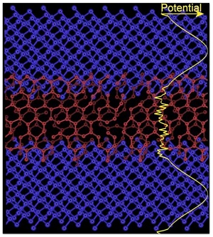
A schematic atomic diagram of a quantum well made from amorphous carbon layers. The blue atoms represent amorphous carbon with a high percentage of diamond-like carbon. The maroon atoms represent amorphous carbon which is graphite-like. The diamond-like regions have a high potential (diamond is insulating) while the graphite-like regions are more metallic. This creates a quantum well as electrons are confined within the graphite-like region due to the relatively high potential in the diamond-like regions. Superlattices are made up of a series of quantum wells. (Image: Wits University)
The group, headed by Professor Somnath Bhattacharyya has been working for the past 10 years on developing carbon-based nano-electronic devices.
"Carbon is the future in the electronics field and it soon will be challenging many other semiconductors, including silicon," says Bhattacharyya.
The physics of carbon superlattices is more complex than that of crystalline superlattices (such as gallium arsenide), since the material is amorphous and carbon atoms tend to form chains and networks. The Wits group, in association with researchers at the University of Surrey in the UK, has developed a detailed theoretical approach to understand the experimental data obtained from carbon devices. The paper has been published in Scientific Reports ("Coherent quantum transport features in carbon superlattice structures").
"This work provides an understanding of the fundamental quantum properties of carbon superlattices, which we can now use to design quantum devices for specific applications," says lead author, Wits PhD student, Ross McIntosh. "Our work provides strong impetus for future studies of the high-frequency electronic and optoelectronic properties of carbon superlattices".
Through their work, the group reported one of the first theoretical models that can explain the fundamental electronic transport properties in disordered carbon superlattices.
Bhattacharyya started looking at the use of carbon for semiconductor applications almost 10 years ago, before he joined Wits University, when he and co-authors from the University of Surrey developed and demonstrated negative differential resistance and excellent high-frequency properties of a quantum device made up of amorphous carbon layers. This work was published in Nature Materials in 2006.
McIntosh undertook the opportunity at honours level to measure the electrical properties of carbon superlattice devices. Now, as a PhD student and having worked extensively with theoretician Dr. Mikhail V. Katkov, he has extended the theoretical framework and developed a technique to calculate the transport properties of these devices.
Bhattacharyya believes this work will have immense importance in developing Carbon-based high-frequency devices.
"It will open not only fundamental studies in Carbon materials, but it will also have industrial applications in the electronic and optoelectronic device sector," he says.
A schematic atomic diagram of a quantum well made from amorphous carbon layers. The blue atoms represent amorphous carbon with a high percentage of diamond-like carbon. The maroon atoms represent amorphous carbon which is graphite-like. The diamond-like regions have a high potential (diamond is insulating) while the graphite-like regions are more metallic. This creates a quantum well as electrons are confined within the graphite-like region due to the relatively high potential in the diamond-like regions. The maroon chains through the diamond-like regions represent polymeric chains, a feature which is unique to carbon superlattices. Superlattices are made up of a series of quantum wells. The green atoms represent nitrogen impurities.
Superlattices are currently used as state of the art high frequency oscillators and amplifiers and are beginning to find use in optoelectronics as detectors and emitters in the terahertz regime. While the high frequency electrical and optoelectronic properties of conventional semiconductors are limited by the dopants used to modify their electronic properties, the properties of superlattices can be tuned over a much wider range to create devices which operate in regimes where conventional devices cannot.
Superlattice electronic devices can operate at higher frequencies and optoelectronic devices can operate at lower frequencies than their conventional counterparts. The lack of terahertz emitters and detectors has resulted in a gap in that region of the electromagnetic spectrum (known as the "terahertz gap"), which is a significant limitation, as many biological molecules are active in this regime. This also limits terahertz radio astronomy.
Amorphous Carbon devices are extremely strong, can operate at high voltages and can be developed in most laboratories in the world, without sophisticated nano-fabrication facilities. New Carbon-based devices could find application in biology, space technology, science infrastructure such as the Square Kilometre Array (SKA) telescope in South Africa, and new microwave detectors.
"What was lacking earlier was an understanding of device modelling. If we have a model, we can improve the device quality, and that is what we now have," says Bhattacharyya.
Share on:


Subscribe
Stay ahead of the technologies shaping the future of electronics with our latest newsletter, Advanced Electronics Packaging Digest. Get expert insights on advanced packaging, materials, and system-level innovation, delivered straight to your inbox.
Subscribe now to stay informed, competitive, and connected.
Suggested Items
I-Connect007 Editor’s Choice: Five Must-Reads for the Week
05/15/2026 | Nolan Johnson, I-Connect007When you work in the news business, even in trade media, you can never really get that far away from it. We never want to miss something important. Chances are, even the books we take on our “vacations” end up having to do with the business. For example, my colleague Michelle Te recommended “Creativity, Inc., by Ed Catmull, a business skills study wrapped up in stories about Pixar, which I brought with me on a trip through the stunning U.S. Mountain West. Now, I’m back, and here are my recommendations for the week.
Incap India Invests in Testing and SMT Upgrades to Scale Production
05/15/2026 | IncapIncap India has completed the installation of a new flying probe test system and a full SMT (Surface-Mount Technology) line upgrade at its Tumkur factory.
Interlink Electronics Reports Q1 2026 Results
05/15/2026 | Globe NewswireRevenue for the first quarter of 2026 increased 15% to $3.07 million, compared to $2.66 million in the first quarter of 2025. The increase was driven by higher shipments of the Company’s force-sensing and printed electronics products, partially offset by lower sales of its gas‑sensor products.
New Book Explores How UV Technology Is Transforming Electronics Protection, Efficiency, and Sustainability
05/14/2026 | I-Connect007I-Connect007 proudly announces the recent release of The Printed Circuit Designer’s Guide to…™ UV Curable Conformal Coatings. Authored by respected industry technologists Brian Chislea and Cody Schoener, PhD, of Dow, Inc., this new volume offers a comprehensive exploration of UV-curable conformal coatings and their expanding role in improving the protection, performance, and sustainability of electronic assemblies.
Nortech Systems Reports Q1 Results
05/14/2026 | Globe NewswireNortech Systems Incorporated, a leading provider of engineering and manufacturing solutions for complex electromedical and electromechanical products serving the medical imaging, medical device, industrial, and aerospace & defense markets, reported financial results for the first quarter ended March 31, 2026.