


 Trouble in Your Tank: Understanding Interconnect Defects, Part 1
 It’s Only Common Sense: Marketing Isn’t Fluff, It’s Ammunition
 Driving Innovation: Mechanical and Optical Processes During Rigid-flex Production


Additive Manufacturing: A New Twist for Stretchable Electronics?
January 4, 2017 | Missouri University of Science and TechnologyEstimated reading time: 3 minutes
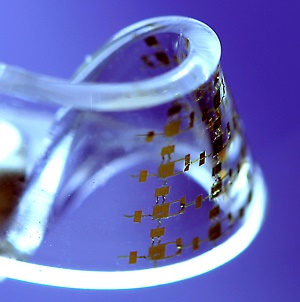
Electronic components that can be elongated or twisted – known as “stretchable” electronics – could soon be used to power electronic gadgets, the onboard systems of vehicles, medical devices and other products. And a 3-D printing-like approach to manufacturing may help make stretchable electronics more prevalent, say researchers at Missouri University of Science and Technology.
New bendable electronic devices like the one pictured above could become more common in the future. Photo by John Rogers, University of Illinois, courtesy of the National Science Foundation.
Writing in the January 2017 edition of the journal Micromachines, Missouri S&T researchers assess the current state of the emerging field of stretchable electronics, focusing on a type of conductor that can be built on or set into the surface of a polymer known as elastomer.
These conductors could one day replace the rigid, brittle circuit board that powers many of today’s electronic devices. They could be used, for example, as wearable sensors that adhere to the skin to monitor heart rate or brain activity, as sensors in clothing or as thin solar panels that could be plastered onto curved surfaces.
Key to the future of stretchable electronics is the surface, or substrate. Elastomer, as its name implies, is a flexible material with high elasticity, which means that it can be bent, stretched, buckled and twisted repeatedly with little impact on its performance.
One challenge facing this class of stretchable electronics involves “overcoming mismatches” between the flexible elastomer base and more brittle electronic conductors, the researchers explain in their paper, “Materials, Mechanics, and Patterning Techniques for Elastomer-Based Stretchable Conductors” (Micromachines 2017, 8(1), 7).
“Unique designs and stretching mechanics have been proposed to harmonize the mismatches and integrate materials with widely different properties as one unique system,” writes the research team, which is led by Dr. Heng Pan, assistant professor of mechanical and aerospace engineering at Missouri S&T.
A relatively new manufacturing technique known as additive manufacturing may help resolve this issue, Pan says.
Additive manufacturing is a process that allows manufacturers to create three-dimensional objects, layer by layer – much like 3-D printing, but with metals, ceramics or other materials. In their paper, the researchers suggest that additive manufacturing could be used to “print” very thin layers of highly conductive materials onto an elastomer surface.
“With the development of additive manufacturing, direct writing techniques are showing up as an alternative to the traditional subtractive patterning methods,” the S&T researchers say.
Subtractive approaches include photolithography, which is commonly used to manufacture semiconductors.
Pan and his colleagues see additive manufacturing as a relatively economical approach to creating these new devices. At Missouri S&T, they are testing an approach that Pan calls “direct aerosol printing.” The process involves spraying a conductive material and integrating with a stretchable substrate to develop sensors that can be placed on skin.
“With the increase of complexity and resolution of devices, higher requirements for patterning techniques are expected,” they write. “Direct printing, as an additive manufacturing method, would satisfy such requirements and offer low cost and high speed in both prototyping and manufacturing. It might be a solution for cost-effective and scalable fabrication of stretchable electronics.”
Yet further challenges must be addressed before stretchable electronics become widely used as components in consumer electronics, medical devices or other fields, the researchers say. These challenges include the development of stretchable batteries that can store energy and the need to ensure that stretchable electronics and the malleable surfaces they’re built upon perform and age well together.
Nevertheless, Pan and his colleagues are optimistic for the future of stretchable electronics. They foresee a growth in the types of materials that could be used as efficient conductors of electricity and as flexible surfaces on which to build stretchable electronics.
Share on:


Testimonial
"Our marketing partnership with I-Connect007 is already delivering. Just a day after our press release went live, we received a direct inquiry about our updated products!"
Rachael Temple - AlltematedSuggested Items
Green Circuits Appoints Kaitlyn Muhlenforth as Marketing Manager
11/05/2025 | Green CircuitsGreen Circuits, a full-service Electronics Manufacturing Services (EMS) partner to leading OEMs, is excited to announce the appointment of Kaitlyn Muhlenforth as its new Marketing Manager.
Photonics Systems Group Announces Exclusive After-Hours Tech Event at productronica 2025
11/05/2025 | Photonics Systems GroupPhotonics Systems Group (PSG), a leading expert in laser micromachining specifically for the electronics industry, announced its inaugural after-hours technical event, the Photonics Tech Evening, to be held on November 19, 2025, during Productronica 2025.
EMS and ODM Market Size to Surpass USD 1589.62 Billion by 2033, Rising at 7.40% CAGR
11/04/2025 | Globe NewswireAccording to the SNS Insider, “The EMS and ODM market size was valued at USD 900.09 Billion in 2025E and is projected to reach USD 1,589.62 Billion by 2033, growing at a CAGR of 7.40% during 2026–2033.”
New Podcast Episode: “Bonding Innovation: How Adhesives and Coatings Are Powering the Next Generation of Electronics”
11/05/2025 | I-Connect007I-Connect007 has released of a new episode in its Voices of the Industry podcast series, titled “Bonding Innovation: How Adhesives and Coatings Are Powering the Next Generation of Electronics.” Hosted by Nolan Johnson, this insightful discussion dives deep into the evolving world of adhesives and coatings—materials that are redefining performance, reliability, and design in modern electronics manufacturing. Dymax's Doug Katze, a leading expert in adhesive technologies, delivers what can only be described as a master class on how these critical materials are adapting to meet rapidly changing market demands.
Electronics Manufacturing Powers U.S. Growth, Supporting 5.2 Million Jobs and $1.8 Trillion in Output
11/03/2025 | Global Electronics AssociationNew report from Global Electronics Association shows electronics industry contributes $853 billion to GDP and delivers average annual wages exceeding $156,000, reinforcing its role as a pillar of U.S. economic resilience.