


 The Right Approach: Get Ready for ISO 9001 Version 6
 Dan’s Biz Bookshelf: ‘Still Broke: Walmart’s Remarkable Transformation'
 Driving Innovation: Depth Routing Processes—Achieving Unparalleled Precision in Complex PCBs


Coffee-Ring Effect Leads to Crystallization Control in Semiconductors
March 9, 2017 | KAUSTEstimated reading time: 2 minutes
A chance observation of crystals forming a mark that resembled the stain of a coffee cup left on a table has led to the growth of customized polycrystals with implications for faster and more versatile semiconductors.
Thin-film semiconductors are the foundation of a vast array of electronic and optoelectronic devices. They are generally fabricated by crystallization processes that yield polycrystals with a chaotic mix of individual crystals of different orientations and sizes.
Significant advances in controlling crystallization has been made by a team led by Professor Aram Amassian of Material Science and Engineering at KAUST. The group included individuals from the KAUST Solar Center and others from the University’s Physical Science and Engineering Division in collaboration with Cornell University. Amassian said, “There is no longer a need to settle for random and incoherent crystallization.”
The team’s recent discovery began when Dr. Liyang Yu of the KAUST team noticed that a droplet of liquid semiconductor material dried to form an outer coffee-ring shape that was much thicker than the material at the center. When he induced the material to crystallize, the outer ring crystallized first.
“This hinted that local thickness matters for initiating crystallization,” said Amassian, which went against the prevailing understanding of how polycrystal films form.
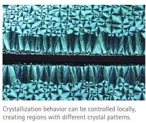
This anomaly led the researchers to delve deeper. They found that the thickness of the crystallizing film could be used to manipulate the crystallization of many materials (see top image). Most crucially, tinkering with the thickness also allowed fine control over the position and orientation of the crystals in different regions of a semiconductor.
“We discovered how to achieve excellent semiconductor properties everywhere in a polycrystal film,” said Amassian. He explained that seeding different patterns of crystallization at different locations also allowed the researchers to create bespoke arrays that can now be used in electronic circuits.
This is a huge improvement to the conventional practice of making do with materials whose good properties are not sustained throughout the entire polycrystal nor whose functions at different regions can be controlled.
“We can now make customized polycrystals on demand,” Amassian said.
Amassian hopes that this development will lead to high-quality, tailored polycrystal semiconductors to promote advances in optoelectronics, photovoltaics and printed electronic components. The method has the potential to bring more efficient consumer electronic devices, some with flexible and lightweight parts, new solar power generating systems and advances in medical electronics. And all thanks to the chance observation of an odd pattern in a semiconductor droplet.
The team will now explore ways to move their work beyond the laboratory through industry partnerships and research collaborations.
Share on:


Testimonial
"Our marketing partnership with I-Connect007 is already delivering. Just a day after our press release went live, we received a direct inquiry about our updated products!"
Rachael Temple - AlltematedSuggested Items
Smartphone Production Rises 4% QoQ in 2Q25 as Inventory Adjustment Ends
09/12/2025 | TrendForceTrendForce’s latest investigations reveal that global smartphone production reached 300 million units in 2Q25, up 4% QoQ and 4.8% YoY, driven by seasonal demand and the recovery of brands such as Oppo and Transsion following inventory adjustments.
I-Connect007 Editor’s Choice: Five Must-Reads for the Week
09/12/2025 | Marcy LaRont, I-Connect007We may be post-Labor Day, but it is still hot-hot-hot here in the great state of Arizona—much like our news cycles, which have continued to snap, crackle, and pop with eye-raising headlines over this past week. In broader global tech news this week, AI and tariff-type restrictions continues to dominate with NVIDIA raising its voice against U.S. lawmakers pushing chip restrictions, ASML investing in a Dutch AI start-up company to the tune of $1.5 billion, and the UAE joining the ranks of the U.S. and China in embracing “open source” with their technology in hopes of accelerating their AI position.
Delta Electronics Posts 26.7% Growth in Sales Revenues for August
09/12/2025 | Delta ElectronicsDelta Electronics, Inc. announced its consolidated sales revenues for August 2025 totaled NT$47,860 million, a 26.7 percent increase as compared to NT$37,770 million for August 2024 and a 5.4 percent increase as compared to NT$45,397 million for July 2025.
Flex Named to TIME's World's Best Companies List for Third Consecutive Year
09/12/2025 | FlexFlex announced its inclusion on the TIME World's Best Companies 2025 list. This marks the third consecutive year the company was included in this prestigious ranking, which recognizes top-performing companies across the globe.
Direct Imaging System Market Size to Hit $4.30B by 2032, Driven by Increasing Demand for High-Precision PCB Manufacturing
09/11/2025 | Globe NewswireAccording to the SNS Insider, “The Direct Imaging System Market size was valued at $2.21 Billion in 2024 and is projected to reach $4.30 Billion by 2032, growing at a CAGR of 8.68% during 2025-2032.”