


 It’s Only Common Sense: Marketing Isn’t Fluff, It’s Ammunition
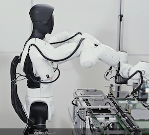
 Driving Innovation: Mechanical and Optical Processes During Rigid-flex Production
 The Chemical Connection: Onshoring PCB Production—Daunting but Certainly Possible


Tarnish-Proof Films for Flexible Displays, Touch Screens, Metamaterials
March 22, 2017 | University of MichiganEstimated reading time: 4 minutes
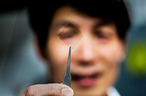
The thinnest, smoothest layer of silver that can survive air exposure has been laid down at the University of Michigan, and it could change the way touchscreens and flat or flexible displays are made.
University of Michigan researchers have created a transparent silver film that could be used in touchscreens, flexible displays and other advanced applications. L. Jay Guo, professor of electrical engineering and computer science, holds up a piece of the material. Image credit: Joseph Xu/Michigan Engineering.
It could also help improve computing power, affecting both the transfer of information within a silicon chip and the patterning of the chip itself through metamaterial superlenses.
By combining the silver with a little bit of aluminum, the U-M researchers found that it was possible to produce exceptionally thin, smooth layers of silver that are resistant to tarnishing. They applied an anti-reflective coating to make one thin metal layer up to 92.4 percent transparent.
The team showed that the silver coating could guide light about 10 times as far as other metal waveguides—a property that could make it useful for faster computing. And they layered the silver films into a metamaterial hyperlens that could be used to create dense patterns with feature sizes a fraction of what is possible with ordinary ultraviolet methods, on silicon chips, for instance.
Screens of all stripes need transparent electrodes to control which pixels are lit up, but touchscreens are particularly dependent on them. A modern touch screen is made of a transparent conductive layer covered with a nonconductive layer. It senses electrical changes where a conductive object—such as a finger—is pressed against the screen.
"The transparent conductor market has been dominated to this day by one single material," said L. Jay Guo, professor of electrical engineering and computer science.
This material, indium tin oxide, is projected to become expensive as demand for touch screens continues to grow; there are relatively few known sources of indium, Guo said.
"Before, it was very cheap. Now, the price is rising sharply," he said.
The ultrathin film could make silver a worthy successor.
L. Jay Guo, professor of electrical engineering and computer science at the University of Michigan, and Chengang Ji, a doctoral student in the same department, discuss results from a test of a "stainless" silver film that their research group has created. Image credit: Joseph Xu/Michigan Engineering
Usually, it's impossible to make a continuous layer of silver less than 15 nanometers thick, or roughly 100 silver atoms. Silver has a tendency to cluster together in small islands rather than extend into an even coating, Guo said.
By adding about 6 percent aluminum, the researchers coaxed the metal into a film of less than half that thickness—seven nanometers. What's more, when they exposed it to air, it didn't immediately tarnish as pure silver films do. After several months, the film maintained its conductive properties and transparency. And it was firmly stuck on, whereas pure silver comes off glass with Scotch tape.
In addition to their potential to serve as transparent conductors for touch screens, the thin silver films offer two more tricks, both having to do with silver's unparalleled ability to transport visible and infrared light waves along its surface. The light waves shrink and travel as so-called surface plasmon polaritons, showing up as oscillations in the concentration of electrons on the silver's surface.
Those oscillations encode the frequency of the light, preserving it so that it can emerge on the other side. While optical fibers can't scale down to the size of copper wires on today's computer chips, plasmonic waveguides could allow information to travel in optical rather than electronic form for faster data transfer. As a waveguide, the smooth silver film could transport the surface plasmons over a centimeter—enough to get by inside a computer chip.
The plasmonic capability of the silver film can also be harnessed in metamaterials, which handle light in ways that break the usual rules of optics. Because the light travels with a much shorter wavelength as it moves along the metal surface, the film alone acts as a superlens. Or, to make out even smaller features, the thin silver layers can be alternated with a dielectric material, such as glass, to make a hyperlens.
Such lenses can image objects that are smaller than the wavelength of light, which would blur in an optical microscope. It can also enable laser patterning—such as is used to etch transistors into silicon chips today—to achieve smaller features.
The first author is Cheng Zhang, a recent U-M doctoral graduate in electrical engineering and computer science who now works as a postdoctoral researcher at National Institute of Standards and Technology.
A paper on this research, titled "High-performance Doped Silver Films: Overcoming Fundamental Material Limits for Nanophotonic Applications" is published in Advanced Materials. The study was supported by the National Science Foundation and the Beijing Institute of Collaborative Innovation. U-M has applied for a patent and is seeking partners to bring the technology to market.
Share on:


Testimonial
"In a year when every marketing dollar mattered, I chose to keep I-Connect007 in our 2025 plan. Their commitment to high-quality, insightful content aligns with Koh Young’s values and helps readers navigate a changing industry. "
Brent Fischthal - Koh YoungSuggested Items
WestDev Announces Advanced Thermal Analysis Integration for Pulsonix PCB Design Suite
10/29/2025 | WestDev Ltd.Pulsonix, the industry-leading PCB design software from WestDev Ltd., announced a major enhancement to its design ecosystem: a direct interface between Pulsonix and ADAM Research's TRM (Thermal Risk Management) analysis software.
Designers Notebook: Power and Ground Distribution Basics
10/29/2025 | Vern Solberg -- Column: Designer's NotebookThe principal objectives to be established during the planning stage are to define the interrelationship between all component elements and confirm that there is sufficient surface area for placement, the space needed to ensure efficient circuit interconnect, and to accommodate adequate power and ground distribution.
Episode 6 of Ultra HDI Podcast Series Explores Copper-filled Microvias in Advanced PCB Design and Fabrication
10/15/2025 | I-Connect007I-Connect007 has released Episode 6 of its acclaimed On the Line with... American Standard Circuits: Ultra High Density Interconnect (UHDI) podcast series. In this episode, “Copper Filling of Vias,” host Nolan Johnson once again welcomes John Johnson, Director of Quality and Advanced Technology at American Standard Circuits, for a deep dive into the pros and cons of copper plating microvias—from both the fabricator’s and designer’s perspectives.
Nolan’s Notes: Tariffs, Technologies, and Optimization
10/01/2025 | Nolan Johnson -- Column: Nolan's NotesLast month, SMT007 Magazine spotlighted India, and boy, did we pick a good time to do so. Tariff and trade news involving India was breaking like a storm surge. The U.S. tariffs shifted India from one of the most favorable trade agreements to the least favorable. Electronics continue to be exempt for the time being, but lest you think that we’re free and clear because we manufacture electronics, steel and aluminum are specifically called out at the 50% tariff levels.
MacDermid Alpha & Graphic PLC Lead UK’s First Horizontal Electroless Copper Installation
09/30/2025 | MacDermid Alpha & Graphic PLCMacDermid Alpha Electronics Solutions, a leading supplier of integrated materials and chemistries to the electronics industry, is proud to support Graphic PLC, a Somacis company, with the installation of the first horizontal electroless copper metallization process in the UK.