


 Trouble in Your Tank: Implementing Direct Metallization in Advanced Substrate Packaging
 It’s Only Common Sense: Storytelling That Sells—Stop Pitching, Start Painting Pictures
 The Right Approach: Get Ready for ISO 9001 Version 6


Invention May Give Spacecraft Improved Damage Report
March 27, 2017 | NASAEstimated reading time: 3 minutes
There are few ways for astronauts to know exactly when the outside of their spacecraft has been damaged, but that may change in the future with an invention that acts like a sensory skin to pick up signs of damage in real-time. The invention uses a series of several technologies to create circuits printed on thin layers and that can be embedded in a spacecraft's structure, scientists behind the invention said.
If successfully incorporated, the innovation could also be applied to a host of satellites, aircraft and even habitats on other worlds.
Micrometeoroids and orbital debris pose threats to spacecraft as they travel at speeds of 17,500 mph in low-Earth orbit, and 24,000+ mph for trips to the moon and deep space. As space shuttle windows revealed, something as small as a paint chip moving at that velocity can punch through several layers of glass.
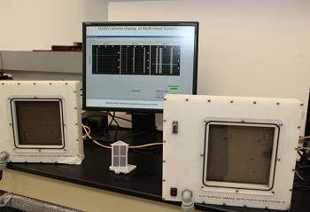
Under development at NASA's Kennedy Space Center in Florida, the Flexible Damage Detection System technology has been pursued as a possible solution to NASA's problem of figuring out in real-time where a spacecraft is damaged and how seriously.
If something pierces a spacecraft's hull – or the first layer or two - there are very limited ways for astronauts aboard a spacecraft to know there might be damage. An impact that goes all the way through and causes a leak would set off alarms, but otherwise the current methods to detect damage require either a camera inspection or a spacewalking astronaut. Nor is there a precise way to pinpoint exactly in real-time where the damage occurred if not visible to the eye or camera so astronauts can assess it.
"I kind of look at it like a sensory skin," said Martha Williams, the scientist leading the development team. "It's a sensory system that tells us where we are damaged and the level of intensity."
The sensory system comprises several systems from low-voltage electric to circuits printed on Kapton thermal insulation film to unique software that tracks the damage.
"There are a lot of technology systems that we leveraged for this," said fellow inventor Tracy Gibson, a scientist with Vencore.
A big part of the work also includes making the manufacturing methods more efficient so the technology can more easily transfer to commercial companies for potential use, Williams said.
Right now for development and demonstration on the ground, the largest square of sensory panel is 6-by-6 inches and it's connected to wiring and a computer that monitors the system. Scientists and engineers envision tiling the squares together like a quilt to make a complete sensor network. They could be foldable and could be used in an inflatable or expandable spacecraft in the future.
Depending on the approach, a spacecraft could have a detection layer wrapping it completely, or just covering a certain area over a particularly critical system.
"It's tailorable, so it can be designed to the specifications of the end user," Gibson said Gibson. "You can tailor it to detect small damages or to pick up large damages and depth of damage."
The damage detector could also be applied to the outside of a habitat on the lunar or Martian surface to calculate damage from small impacts. On Earth, the system could perhaps also be applied to the outside of airplanes to tell pilots when their airframe has been impacted and may be compromised.
In fact, one of the sensor's early tests saw it demonstrated on the outside of a habitat module prototype for a mission simulation that took place in Flagstaff, Arizona. Depending on funding, the team hopes to perform more tests and build new prototypes that continue to advance the concept closer to a system that can be flight tested and then applied to future spacecraft designs.
"We want to bring solutions to NASA's problems," Williams said. "We like to solve problems, I don't think we can even stop inventing, it's how we think. It's who we are."
Share on:


Testimonial
"Our marketing partnership with I-Connect007 is already delivering. Just a day after our press release went live, we received a direct inquiry about our updated products!"
Rachael Temple - AlltematedSuggested Items
I-Connect007 Launches Advanced Electronics Packaging Digest
09/15/2025 | I-Connect007I-Connect007 is pleased to announce the launch of Advanced Electronics Packaging Digest (AEPD), a new monthly digital newsletter dedicated to one of the most critical and rapidly evolving areas of electronics manufacturing: advanced packaging at the interconnect level.
VIDEOTON EAS's Bulgarian Subsidiary Expands Into Automotive Products
09/15/2025 | VideotonVEAS Bulgaria, engaged in electronics manufacturing, has joined the ranks of VIDEOTON companies authorized to produce automotive products.
Variosystems Strengthens North American Presence with Southlake Relaunch 2025
09/15/2025 | VariosystemsVariosystems celebrated the relaunch of its U.S. facility in Southlake, Texas. After months of redesign and reorganization, the opening marked more than just the return to a modernized production site—it was a moment to reconnect with our teams, partners, and the local community.
Hanwha Aerospace to Collaborate with BAE Systems on Advanced Anti-jamming GPS for Guided Missiles
09/15/2025 | HanwhaHanwha Aerospace has signed a contract with BAE Systems to integrate next-generation, anti-jamming Global Positioning System (GPS) technology into Hanwha Aerospace’s Deep Strike Capability precision-guided weapon system.
EV Group Achieves Breakthrough in Hybrid Bonding Overlay Control for Chiplet Integration
09/12/2025 | EV GroupEV Group (EVG), a leading provider of innovative process solutions and expertise serving leading-edge and future semiconductor designs and chip integration schemes, today unveiled the EVG®40 D2W—the first dedicated die-to-wafer overlay metrology platform to deliver 100 percent die overlay measurement on 300-mm wafers at high precision and speeds needed for production environments. With up to 15X higher throughput than EVG’s industry benchmark EVG®40 NT2 system designed for hybrid wafer bonding metrology, the new EVG40 D2W enables chipmakers to verify die placement accuracy and take rapid corrective action, improving process control and yield in high-volume manufacturing (HVM).