


 Trouble in Your Tank: Organic Addition Agents in Electrolytic Copper Plating
 Marcy’s Musings: Can You Hear the Voices?
 Facing the Future: Successfully Navigating the Uncertain Path Ahead


200mm Fabs Thriving; SEMI’s Updated 200mm Fab Report Now Available
July 14, 2017 | SEMIEstimated reading time: 2 minutes
At SEMICON West in San Francisco, Calif., SEMI issued an update to its 200mm Fab Outlook report, with improved and expanded report forecasting of 200mm fab trends out to 2021. SEMI’s analysts updated information on over 100 facilities, including the latest new facilities and investment projects in China. The extensive new report "Global 200mm Fab Outlook to 2021" by SEMI tracks production, pilot, and R&D 200mm facilities worldwide with special attention on capacity expansions and new facilities.
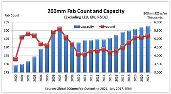
Examining 200mm capacity over the years, the highest level of 200mm capacity was recorded in 2007 and the lowest following this peak in 2009. The capacity decline from 2007 to 2009 was driven by the 2008-2009 global financial crisis, which caused the closure of many facilities, and by the transition of memory and MPU fabrication to 300mm fabs from 200mm.
Since 2009, installed 200mm fab capacity has increased, and by 2020, 200mm capacity is expected to reach almost 5.7 million wafers per month (wpm), and poised to surpass the 2007 peak. According to SEMI’s World Fab Forecast data, by the end of this year, installed capacity will reach close to 5.4 million wpm.
Driven by mobile and wireless applications, IOT, and automotive, the 200mm market is thriving. Many of these products found their niche on 200mm wafers, so companies are expanding capacity in their facilities to the limit, and nine new 200mm facilities are in the pipeline. Looking only at IC volume fabs, the report shows 188 fabs in production in 2016 and expanding to 197 fabs by 2021.China will add most of the 200mm capacity through 2021 with 34 percent growth rate from 2017 to 2021, followed by South East Asia with 29 percent and the Americas with 12 percent.
The Global 200mm Fab Outlook to 2021, published by SEMI in July 2017, includes two files: a 92-page pdf file featuring trend charts, tables and summaries and an Excel file covering 2010 to 2021 detailing on quarterly basis and fab-by-fab developments. This is the third update since the report was first launched in 2015. Since the last report was published in November 2016, the SEMI analyst team has made 232 changes or updates to 132 fabs. The report tracks over 300 facilities using 200mm wafers from R&D, EPI, LED fabs to volume IC fabs.
About SEMI
SEMI connects nearly 2,000 member companies and 250,000 professionals worldwide annually to advance the technology and business of electronics manufacturing. SEMI members are responsible for the innovations in materials, design, equipment, software, and services that enable smarter, faster, more powerful, and more affordable electronic products. Since 1970, SEMI has built connections that have helped its members grow, create new markets, and address common industry challenges together. SEMI maintains offices in Bangalore, Beijing, Berlin, Brussels, Grenoble, Hsinchu, Seoul, Shanghai, Silicon Valley (Milpitas, Calif.), Singapore, Tokyo, and Washington, D.C.
Share on:


Suggested Items
I-Connect007 Editor’s Choice: Five Must-Reads for the Week
04/18/2025 | Andy Shaughnessy, Design007 MagazineIt’s been a busy week in our industry. Never a dull moment! If you’ve been paying attention to our tariff tumult with China and its effect on the stock market, especially if your company does a lot of business with China, you might be tempted to call in a Xanax refill about now. But hang tight. This is still early in the first quarter. This brouhaha serves to underscore our need to manufacture critical laminates and components in the U.S. In this week’s must-reads, we have a potpourri of articles covering tariffs, the next generation of HDI, the three-year anniversary of IPC Mexico, a novel green technology, and emerging design trends.
Real Time with... IPC APEX EXPO 2025: Aster–Enhancing Design for Effective Testing Strategies
04/18/2025 | Real Time with...IPC APEX EXPOWill Webb, technical director at Aster, stresses the importance of testability in design, emphasizing early engagement to identify testing issues. This discussion covers the integration of testing with Industry 4.0, the need for good test coverage, and adherence to industry standards. Innovations like boundary scan testing and new tools for cluster testing are introduced, highlighting advancements in optimizing testing workflows and collaboration with other tools.
IPC President’s Award: Xaver Feiner
04/17/2025 | Nolan Johnson, SMT007 MagazineThroughout his career, Xaver Feiner, vice president of marketing and sales at Zollner Elektronik, has developed extensive expertise in account management and new business development with a strong focus on the semiconductor industry, aerospace, and industrial electronics. Xaver has cultivated a profound understanding of global markets and remains deeply engaged with the challenges and opportunities presented by digital transformation. Since 2020, he has been an active member of the IPC Europe Advocacy Group, where he is dedicated to advancing the position of the electronics industry and the EMS sector across Europe.
New High Power 3D AXI for Power Electronics from Test Research, Inc.
04/17/2025 | TRITest Research, Inc. (TRI), a leading provider of Test and Inspection solutions for the electronics manufacturing industry, proudly announces the launch of the 3D AXI TR7600HP system. Designed for power semiconductor inspection, the TR7600HP enhances accuracy and efficiency in detecting defects in components such as IGBTs, MOSFETs, SiC inverters, and Paladin Connectors.
IPC APEX EXPO 2025 Learning Lounge: Education on the Show Floor
04/16/2025 | Andy Shaughnessy, Design007The conference portion of IPC APEX EXPO has been providing educational opportunities for attendees since the first show. But recently, show managers decided to expand education onto the show floor.