


 The Chemical Connection: Onshoring PCB Production—Daunting but Certainly Possible
 Marcy’s Musings: The Legislative Outlook—Helping or Hurting?
 It’s Only Common Sense: The Phone Is Still Mightier Than the Keyboard


Epec Now Offering PCB Layout and Design Services
July 21, 2017 | EpecEstimated reading time: 1 minute
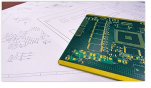
Epec Engineered Technologies, one of America’s oldest printed circuit board (PCB) manufacturers located outside of Boston, Massachusetts, is now offering PCB layout and design services to their customers.
Founded in 1952, Epec has a long history with circuit boards and the PCB industry. Over the past 65 years, Epec has worked on countless circuit board parts for some of the top tier OEMs in the electronics industry. From having PCBs on the Apollo 11 spaceflight, which landed the first humans on the Moon, to their recent advancements in heavy and extreme copper circuit boards, Epec’s sixty-five year history of innovation has truly made them a thought leader amongst the electronics community.
Ed McMahon, CEO of Epec, said, “We have been offering PCB layout and design services a while now, we just never had a large demand for it. In the past when a customer came to us looking for PCB design help, we wouldn’t turn them away; it was just not an advertised offering in our product line.”
Epec’s PCB layout and design services encompass a full design flow including rules driven designs, schematic capture, library development, database construction and verification, signal integrity/design verification, EMI checking and many others.
McMahon added, “We are now seeing more and more companies come to us to help them with their circuit board layout needs. Having the resources in-house allows us to be an extension of our customers engineering teams. We’ve also seen the benefits of customers having their PCB layout and design done by the same company that will be manufacturing their boards as it helps to reduce cost by only designing exactly what they need.”
As Epec continues to expand their PCB supply chain and services, they do so with one goal in mind; to provide their valued customers what they need and when they need it.
About Epec, LLC
Epec Engineered Technologies is the ideal choice for an OEM seeking customized product solutions from a focused and agile partner having supported over 5,000 customers across all sectors of the electronics industry. By providing highly experienced technical resources, a proven manufacturing platform and the fastest delivery in the industry, we are able to provide cost effective and innovative solutions that deliver the highest reliability products to the market faster. Click here for more information.
Share on:


Testimonial
"Your magazines are a great platform for people to exchange knowledge. Thank you for the work that you do."
Simon Khesin - Schmoll MaschinenSuggested Items
Episode 6 of Ultra HDI Podcast Series Explores Copper-filled Microvias in Advanced PCB Design and Fabrication
10/15/2025 | I-Connect007I-Connect007 has released Episode 6 of its acclaimed On the Line with... American Standard Circuits: Ultra High Density Interconnect (UHDI) podcast series. In this episode, “Copper Filling of Vias,” host Nolan Johnson once again welcomes John Johnson, Director of Quality and Advanced Technology at American Standard Circuits, for a deep dive into the pros and cons of copper plating microvias—from both the fabricator’s and designer’s perspectives.
Nolan’s Notes: Tariffs, Technologies, and Optimization
10/01/2025 | Nolan Johnson -- Column: Nolan's NotesLast month, SMT007 Magazine spotlighted India, and boy, did we pick a good time to do so. Tariff and trade news involving India was breaking like a storm surge. The U.S. tariffs shifted India from one of the most favorable trade agreements to the least favorable. Electronics continue to be exempt for the time being, but lest you think that we’re free and clear because we manufacture electronics, steel and aluminum are specifically called out at the 50% tariff levels.
MacDermid Alpha & Graphic PLC Lead UK’s First Horizontal Electroless Copper Installation
09/30/2025 | MacDermid Alpha & Graphic PLCMacDermid Alpha Electronics Solutions, a leading supplier of integrated materials and chemistries to the electronics industry, is proud to support Graphic PLC, a Somacis company, with the installation of the first horizontal electroless copper metallization process in the UK.
Electrodeposited Copper Foils Market to Grow by $11.7 Billion Over 2025-2032
09/18/2025 | Globe NewswireThe global electrodeposited copper foils market is poised for dynamic growth, driven by the rising adoption in advanced electronics and renewable energy storage solutions.
MacDermid Alpha Showcases Advanced Interconnect Solutions at PCIM Asia 2025
09/18/2025 | MacDermid Alpha Electronics SolutionsMacDermid Alpha Electronic Solutions, a global leader in materials for power electronics and semiconductor assembly, will showcase its latest interconnect innovations in electronic interconnect materials at PCIM Asia 2025, held from September 24 to 26 at the Shanghai New International Expo Centre, Booth N5-E30