


 Trouble in Your Tank: Implementing Direct Metallization in Advanced Substrate Packaging
 It’s Only Common Sense: Storytelling That Sells—Stop Pitching, Start Painting Pictures
 The Right Approach: Get Ready for ISO 9001 Version 6


Georgia Tech Researchers Support DARPA’s New 'CHIPS' Initiative
October 5, 2017 | Georgia TechEstimated reading time: 4 minutes
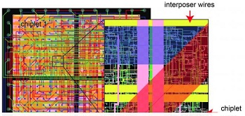
A team of Georgia Tech researchers is bringing electronic design software and communications expertise to DARPA's new CHIPS initiative, which will enable future generations of integrated circuits to be assembled from plug-and-play modules known as “chiplets.” Reusing blocks of existing microelectronics technology could reduce the need to design complex monolithic chips from scratch for new applications.
By allowing components such as memory modules or signal processors to be easily fitted together like the parts of a jigsaw puzzle, the initiative could help reduce the cost of new ICs for Department of Defense (DoD) agencies and accelerate the application of new technology. While the initiative is driven by DoD needs for its ships, tanks and aircraft, innovations developed by the program could also reduce the cost of developing low-volume specialized devices in the commercial world.
“The goal of this program is to make the design more modular so we can reuse existing components, making the design process much faster, easier and cheaper,” said Sung Kyu Lim, a School of Electrical and Computer Engineering professor who heads up Georgia Tech’s part of the initiative. “We’ll be able to create new chips to meet specific needs by reusing these chiplets and putting them together in modular fashion. The modular design will allow us to pick and choose the components we need for specific applications.”
Monolithic integrated circuits like those that go into smartphones contain billions of transistors. They cost tens to hundreds of millions of dollars and take months to design. Companies selling large volumes of consumer products can afford that design cost, but DoD agencies that need smaller numbers of specialized devices are looking for ways to reduce the design cost and time required.
Enter DARPA’s Common Heterogeneous Integration and Intellectual Property Reuse Strategies (CHIPS) effort, which will use interposer technology – a silicon and copper interface – that will interconnect the chiplets. While the interposer adds a level of complexity to the design of the devices, it’s necessary to facilitate the 3-D modular assembly. The chiplets themselves could arise from existing designs, with engineers modifying memory, signal processing and other blocks from ICs already in production.
“Instead of designing a whole new chip, you can borrow from what’s already been designed to put together a new chip quickly and at lower cost,” said Lim, who holds the Dan Fielder Endowed Chair. The chiplets would be assembled and then packaged together, facilitating shorter interconnect lengths that would reduce communication time and energy consumption between the components. The modular nature of the chiplets would also allow a block to be replaced by new technology without redesigning an entire IC.
The four-year CHIPS effort involves 11 teams, including major defense contractors, microelectronics companies, design firms – and two other universities: the University of Michigan and North Carolina State University. In addition to Lim, the Georgia Tech effort will involve three other faculty members: Pippin Chair Professor Madhavan Swaminathan, Professor Saibal Mukhopadhyay and Assistant Professor Tushar Krishna, all from the School of Electrical and Computer Engineering.
About $3.7 million will come to Georgia Tech as part of the project’s budget. In addition to the faculty members, that will fund a research engineer and up to eight graduate students.
The Georgia Tech team will provide electronic design automation software needed to produce the chiplets, develop translator technology that will allow chiplets operating in different languages to communicate, and evaluate different design standards brought to the project by other teams.
- Circuit design tools will be needed to create the chiplets, many of which will be adapted from existing designs. “A big part of what we’ll deliver for this project is electronic design automation (EDA) tools,” said Lim. “We want to automate the entire chiplet generation and integration process as much as possible using algorithms and software tools.”
- Modules from different companies may use different languages. To use them together in a new system, the chiplets will need translators, circuitry and software that will wrap around each chiplet. “We need to understand all the different languages, so we can help the chiplets communicate with one another,” Lim explained. “The complexity will depend on how many interface protocols are used in the system.”
- The project teams will have to work together using the same design standards. Lim’s team will establish tools and techniques for evaluating the different standards now used by different teams that are part of the overall effort. “We will provide a fair means of comparing the different technology options and picking the winner,” said Lim.
Though DARPA’s focus is on providing technology for DoD users, solutions developed from the initiative could also have broad benefits in the commercial microelectronics world. “Small- and medium-sized companies could will benefit a lot from this,” Lim said. “Small design houses that would like to develop their own ICs will likely be very interested.”
Meeting the program’s ambitious goals will be challenging, Lim says, with reliability, power, mechanical and thermal issues on the horizon. “The success of this program will make a significant contribution to the defense industry and the microelectronics community in general,” he said.
Share on:


Testimonial
"Our marketing partnership with I-Connect007 is already delivering. Just a day after our press release went live, we received a direct inquiry about our updated products!"
Rachael Temple - AlltematedSuggested Items
Trouble in Your Tank: Implementing Direct Metallization in Advanced Substrate Packaging
09/15/2025 | Michael Carano -- Column: Trouble in Your TankDirect metallization systems based on conductive graphite are gaining popularity throughout the world. The environmental and productivity gains achievable with this process are outstanding. Direct metallization reduces the costs of compliance, waste treatment, and legal issues related to chemical exposure. A graphite-based direct plate system has been devised to address these needs.
Closing the Loop on PCB Etching Waste
09/09/2025 | Shawn Stone, IECAs the PCB industry continues its push toward greener, more cost-efficient operations, Sigma Engineering’s Mecer System offers a comprehensive solution to two of the industry’s most persistent pain points: etchant consumption and rinse water waste. Designed as a modular, fully automated platform, the Mecer System regenerates spent copper etchants—both alkaline and acidic—and simultaneously recycles rinse water, transforming a traditionally linear chemical process into a closed-loop system.
Driving Innovation: Depth Routing Processes—Achieving Unparalleled Precision in Complex PCBs
09/08/2025 | Kurt Palmer -- Column: Driving InnovationIn PCB manufacturing, the demand for increasingly complex and miniaturized designs continually pushes the boundaries of traditional fabrication methods, including depth routing. Success in these applications demands not only on robust machinery but also sophisticated control functions. PCB manufacturers rely on advanced machine features and process methodologies to meet their precise depth routing goals. Here, I’ll explore some crucial functions that empower manufacturers to master complex depth routing challenges.
Trouble in Your Tank: Minimizing Small-via Defects for High-reliability PCBs
08/27/2025 | Michael Carano -- Column: Trouble in Your TankTo quote the comedian Stephen Wright, “If at first you don’t succeed, then skydiving is not for you.” That can be the battle cry when you find that only small-diameter vias are exhibiting voids. Why are small holes more prone to voids than larger vias when processed through electroless copper? There are several reasons.
The Government Circuit: Navigating New Trade Headwinds and New Partnerships
08/25/2025 | Chris Mitchell -- Column: The Government CircuitAs global trade winds continue to howl, the electronics manufacturing industry finds itself at a critical juncture. After months of warnings, the U.S. Government has implemented a broad array of tariff increases, with fresh duties hitting copper-based products, semiconductors, and imports from many nations. On the positive side, tentative trade agreements with Europe, China, Japan, and other nations are providing at least some clarity and counterbalance.