


 Trouble in Your Tank: In Complex Systems, Design Rules Aren’t Optional
 It’s Only Common Sense: The Phone Is Still Your Competitive Advantage
 Dan’s Biz Bookshelf: ‘The Next RenAIssance: AI and the Expansion of Human Potential’


Paper-based Supercapacitor Uses Metal Nanoparticles to Boost Energy Density
October 9, 2017 | Georgia TechEstimated reading time: 3 minutes
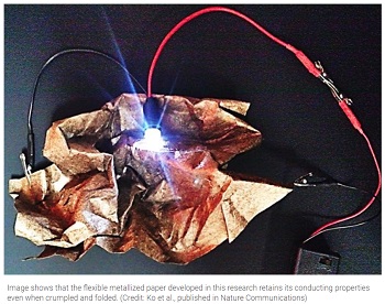
Using a simple layer-by-layer coating technique, researchers from the U.S. and Korea have developed a paper-based flexible supercapacitor that could be used to help power wearable devices. The device uses metallic nanoparticles to coat cellulose fibers in the paper, creating supercapacitor electrodes with high energy and power densities – and the best performance so far in a textile-based supercapacitor.
By implanting conductive and charge storage materials in the paper, the technique creates large surface areas that function as current collectors and nanoparticle reservoirs for the electrodes. Testing shows that devices fabricated with the technique can be folded thousands of times without affecting conductivity.
“This type of flexible energy storage device could provide unique opportunities for connectivity among wearable and internet of things devices,” said Seung Woo Lee, an assistant professor in the Woodruff School of Mechanical Engineering at the Georgia Institute of Technology. “We could support an evolution of the most advanced portable electronics. We also have an opportunity to combine this supercapacitor with energy-harvesting devices that could power biomedical sensors, consumer and military electronics, and similar applications.”
The research, done with collaborators at Korea University, was supported by the National Research Foundation of Korea and reported September 14 in the journal Nature Communications.
Energy storage devices are generally judged on three properties: their energy density, power density and cycling stability. Supercapacitors often have high power density, but low energy density – the amount of energy that can be stored – compared to batteries, which often have the opposite attributes. In developing their new technique, Lee and collaborator Jinhan Cho from the Department of Chemical and Biological Engineering at Korea University set out to boost energy density of the supercapacitors while maintaining their high power output.
They began by dipping paper samples into a beaker of solution containing an amine surfactant material designed to bind the gold nanoparticles to the paper. Next they dipped the paper into a solution containing gold nanoparticles. Because the fibers are porous, the surfactants and nanoparticles enter the fibers and become strongly attached, creating a conformal coating on each fiber.
By repeating the dipping steps, the researchers created a conductive paper on which they added alternating layers of metal oxide energy storage materials such as manganese oxide. The ligand-mediated layer-by-layer approach helped minimize the contact resistance between neighboring metal and/or metal oxide nanoparticles. Using the simple process done at room temperatures, the layers can be built up to provide the desired electrical properties.
“It’s basically a very simple process,” Lee said. “The layer-by-layer process, which we did in alternating beakers, provides a good conformal coating on the cellulose fibers. We can fold the resulting metallized paper and otherwise flex it without damage to the conductivity.”
Though the research involved small samples of paper, the solution-based technique could likely be scaled up using larger tanks or even a spray-on technique. “There should be no limitation on the size of the samples that we could produce,” Lee said. “We just need to establish the optimal layer thickness that provides good conductivity while minimizing the use of the nanoparticles to optimize the tradeoff between cost and performance.”
The researchers demonstrated that their self-assembly technique improves several aspects of the paper supercapacitor, including its areal performance, an important factor for measuring flexible energy-storage electrodes. The maximum power and energy density of the metallic paper-based supercapacitors are estimated to be 15.1 mW/cm2 and 267.3 uW/cm2, respectively, substantially outperforming conventional paper or textile supercapacitors.
The next steps will include testing the technique on flexible fabrics, and developing flexible batteries that could work with the supercapacitors. The researchers used gold nanoparticles because they are easy to work with, but plan to test less expensive metals such as silver and copper to reduce the cost.
During his Ph.D. work, Lee developed the layer-by-layer self-assembly process for energy storage using different materials. With his Korean collaborators, he saw a new opportunity to apply that to flexible and wearable devices with nanoparticles.
“We have nanoscale control over the coating applied to the paper,” he added. “If we increase the number of layers, the performance continues to increase. And it’s all based on ordinary paper.”
In addition to those already mentioned, the research team included Yongmin Ko and Minseong Kwon from Korea University, Wan Ki Bae from the Photoelectronic Hybrids Research Center at the Korea Institute of Science and Technology, and Byeongyong Lee from Georgia Tech.
Share on:


Subscribe
Stay ahead of the technologies shaping the future of electronics with our latest newsletter, Advanced Electronics Packaging Digest. Get expert insights on advanced packaging, materials, and system-level innovation, delivered straight to your inbox.
Subscribe now to stay informed, competitive, and connected.
Suggested Items
Driving Innovation: Selecting the Right Laser Source
04/28/2026 | Simon Khesin -- Column: Driving InnovationWhen I first joined Schmoll Maschinen, I brought experience from almost every PCB process, except for laser. As I immersed myself in laser processing, I realized why it can seem so daunting to a newcomer. The complexity arises from three intersecting factors: A vast variety of laser sources: CO2, UV-nano, green-pico, UV-pico, IR-pico, and others; a diverse range of applications: Drilling, cutting, ablation, and more; and an extensive list of materials: These have vastly different absorption rates. Choosing the right machine or laser source is rarely trivial. Even for experienced engineers, answering "Which source is best?" requires examining the business's specific goals.
Institute of Circuit Technology Spring Seminar 2026: A Bright Future in Europe
04/23/2026 | Pete Starkey, I-Connect007Through the leafy lanes and spring flowers of Warwickshire and back to Meridan, the traditional centre of England, and now officially part of the Metropolitan Borough of Solihull in the county of the West Midlands, I attended the Annual General Meeting and Spring Seminar of the Institute of Circuit Technology (ICT) on April 14. Out of the AGM came notable changes in leadership at the top of the Institute: the retirement of Mat Beadel as chair and Emma Hudson as technical director. Effective May 1, Steve Driver is the new chair, and Alun Morgan is the new technical director.
ACCM Unveils Negative and Near-zero CTE Materials for Large-Format AI Chips
04/21/2026 | Advanced Chip and Circuit MaterialsAdvanced Chip and Circuit Materials, Inc. (ACCM) has launched two new materials: Celeritas HM50, with a negative coefficient of thermal expansion (CTE) of -8 ppm/°C to offset the positive CTE and expansion of copper with temperature on circuit boards, and Celeritas HM001, with near-zero CTE and the low-loss performance needed for high-speed signal layers to 224 Gb/s and faster in artificial intelligence (AI) circuits.
Fresh PCB Concepts: Designing PCBs for Harsh Environments—Reliability Is Engineered Upstream
04/23/2026 | Team NCAB -- Column: Fresh PCB ConceptsWhen engineers hear the phrase “harsh environment,” they usually think of the extreme temperature swings, vibration and shock, pressure changes, or radiation in aerospace. However, aerospace is not the only harsh environment where electronic assemblies must survive. Automotive power electronics, downhole oil and gas tools, marine controls, rail systems, defense platforms, and industrial automation equipment all expose PCBs to environments that are equally unforgiving. The stress mechanisms may differ, but the physics does not.
Advanced Packaging for AI: Reliability Starts at the Cu/Cu/Cu Microvia Junction
04/20/2026 | Kuldip Johal, MKS' AtotechThe rapid growth of AI computing, from training clusters to inference at scale, is reshaping demand across the entire electronics supply chain. Advances in technology requirements, such as higher bandwidth, lower latency, and greater compute density, are driving the development of advanced packaging technologies and transforming the PCB industry across design, manufacturing, testing, and even architecture.