


 The Right Approach: Get Ready for ISO 9001 Version 6
 Dan’s Biz Bookshelf: ‘Still Broke: Walmart’s Remarkable Transformation'
 Driving Innovation: Depth Routing Processes—Achieving Unparalleled Precision in Complex PCBs


Biodegradable Electronics
October 13, 2017 | Fraunhofer FEPEstimated reading time: 1 minute
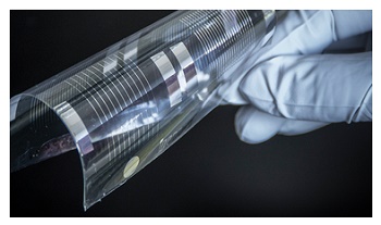
Under the direction of the Fraunhofer Institute for Organic Electronics, Electron Beam and Plasma Technology FEP, an in-house Fraunhofer project for development of biodegradable electronics was begun last year. The Fraunhofer Institute for Electronic Nano Systems ENAS, the Fraunhofer Institute for Biomedical Engineering IBMT, the Fraunhofer Institute for Silicate Research ISC, and the Fraunhofer Resource Recycling and Strategy Project Group IWKS are working together on the project.
Electronic components that are completely broken down in a biological environment after a pre-defined operating life open up novel applications as well as ways for reducing their ecological footprint.
One enabling technology for such components is the manufacture of biodegradable conductive traces on biodegradable substrates using vacuum technologies. This technology was developed by Fraunhofer FEP.
A novel application area for these innovative electronic components for example is in the field of active medical implants that after expiration of their operating life are resorbed by tissue, thereby sparing the patient a second surgical intervention.
The Fraunhofer Gesellschaft e. V. is now funding the "bioElektron - Biodegradable Electronics for Active Implants" project through its in-house program (funding No. MAVO B31 301). The goal of the project is the development of essential components for biodegradable electronic parts that can be employed for example in an implant.
This includes in particular:
- biodegradable conductor structures
- biodegradable electrodes for collecting electrical signals or delivering electrical stimulation
- biodegradable thin-film transistors and circuitry
- biodegradable barrier coatings as moisture and gas barriers, and electrical insulation layers
These elements will be monolithically integrated into a flexible thin-film device.
Conductor structures and organic thin-film transistors are being developed at Fraunhofer FEP using vacuum technology. Deposition of magnesium via thermal evaporation under high vacuum conditions is being used as an enabling technology for this purpose. Magnesium is known for being a biodegradable and biologically compatible metal that is already employed in clinical environments as an absorbable implant material. The challenge consists of depositing this metal upon biodegradable polymer films that magnesium does not adhere sufficiently to under normal process control. By suitably pre-treating the substrates using a combination of drying, plasma treatment, and utilization of seed layers, finely structured high-quality conductor structures were able to be produced.
Share on:


Testimonial
"Our marketing partnership with I-Connect007 is already delivering. Just a day after our press release went live, we received a direct inquiry about our updated products!"
Rachael Temple - AlltematedSuggested Items
United Electronics Corporation Unveils Revolutionary CIMS Galaxy 30 Automated Optical Inspection System
09/11/2025 | United Electronics CorporationUnited Electronics Corporation (UEC) today announced the launch of its new groundbreaking CIMS Galaxy 30 Automated Optical Inspection (AOI) machine, setting a new industry standard for precision electronics manufacturing quality control. The Galaxy 30, developed and manufactured by CIMS, represents a significant leap forward in inspection technology, delivering exceptional speed improvements and introducing cutting-edge artificial intelligence capabilities.
Intel Announces Key Leadership Appointments to Accelerate Innovation and Strengthen Execution
09/09/2025 | Intel CorporationIntel Corporation today announced a series of senior leadership appointments that support the company’s strategy to strengthen its core product business, build a trusted foundry, and foster a culture of engineering across the business.
DARPA, State of New Mexico Establish Framework to Advance Quantum Computing
09/08/2025 | DARPAAs part of the Quantum Benchmarking Initiative (QBI), DARPA signed an agreement with the State of New Mexico’s Economic Development Department to create the Quantum Frontier Project.
LPKF Strengthens LIDE Technology Leadership with New Patent Protection in Korea
09/04/2025 | LPKFLPKF Laser & Electronics SE today announced that its groundbreaking LIDE (Laser Induced Deep Etching) technology has received additional patent protection in Korea through the Korean Patent Office (KPCA), effective September 1, 2025.
UHDI Fundamentals: UHDI Technology and Industry 4.0
09/03/2025 | Anaya Vardya, American Standard CircuitsUltra high density interconnect (UHDI) technology is rapidly transforming how smart systems are designed and deployed in the context of Industry 4.0. With its capacity to support highly miniaturized, high-performance, and densely packed electronics, UHDI is a critical enabler of the smart, connected, and automated industrial future. Here, I’ll explore the synergy between UHDI and Industry 4.0 technologies, highlighting applications, benefits, and future directions.