


 Happy’s Tech Talk #44: Memories of the ‘Mystery Systems of the East’
 The Right Approach: Electro-Tek—A Williams Family Legacy, Part 2
 Alpha Insights, Performance by Design: Understanding Heat at the Core of Every Design


Think Laterally to Sidestep Production Problems
October 16, 2017 | KAUSTEstimated reading time: 2 minutes
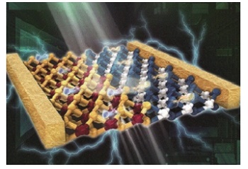
Super thin photovoltaic devices underpin solar technology and gains in the efficiency of their production are therefore keenly sought. KAUST researchers have combined and rearranged different semiconductors to create so-called lateral p-n heterojunctions—a simpler process they hope will transform the fabrication of solar cells, self-powered nanoelectronics as well as ultrathin, transparent, flexible devices.
Two-dimensional semiconductor monolayers, such as graphene and transition-metal dichalcogenides like WSe2 and MoS2, have unique electrical and optical properties that make them potential alternatives to conventional silicon-based materials. Recent advances in material growth and transfer techniques have allowed scientists to manipulate these monolayers. Specifically, vertical stacking has led to ultrathin photovoltaic devices but requires multiple complex transfer steps. These steps are hampered by various issues, such as the formation of contaminants and defects at the monolayer interface, which limit device quality.
“Devices obtained using these transfer techniques are usually unstable and vary from sample to sample,” says lead researcher and former visiting student of Associate Professor, Jr-Hau He, Meng-Lin Tsai, who adds that transfer-related contaminants significantly affect device reliability. Electronic properties have also proven difficult to control by vertical stacking.
To fully harness the exceptional properties of these two-dimensional materials, Tsai’s team, under the mentorship of He, created monolayers featuring lateral WSe2–MoS2 heterojunctions and incorporated them into solar cells. Under simulated sunlight, the cells achieved greater power conversion efficiency than their vertically stacked equivalents.
To do this, first the researchers synthesized the heterojunctions by consecutively depositing WSe2 and MoS2 on a sapphire substrate. Next, they transferred the materials onto a silicon-based surface for photovoltaic device fabrication.
High-resolution microscopy revealed that the lateral junction displayed a clear separation between the semiconductors at the interface. Also, the researchers detected no discernable height difference between semiconductor regions, consistent with an atomically thin interface.
These interfacial characteristics signaled success. “Our structures are cleaner and more ideal than vertically stacked assemblies because we didn’t need the multi-step transfer procedure,” explains Tsai.
Furthermore, the lateral heterojunctions mostly retained their efficiency despite changes to the orientation of the incident light. Being able to take light coming from any direction means expensive solar tracking systems will become redundant.
According to Tsai, the implementation of lateral heterojunctions in more complex circuits and interconnects may result in higher performance than in conventional solar cells and so the team is working on the next steps. “We are trying to understand the underlying kinetics and thermodynamics of these heterojunctions to design more efficient cells," he adds.
Share on:


Testimonial
"The I-Connect007 team is outstanding—kind, responsive, and a true marketing partner. Their design team created fresh, eye-catching ads, and their editorial support polished our content to let our brand shine. Thank you all! "
Sweeney Ng - CEE PCBSuggested Items
The Impact of the AI Boom on PCB and Raw Materials Supply Chains
11/13/2025 | Mark Goodwin, Ventec International GroupThe PCB industry is entering a period of unprecedented structural change, driven by the demands of artificial intelligence and advanced computing. What was once a cyclical market has become a capacity race. It’s one that rewards foresight, collaboration, and strategic supply partnerships. Understanding these dynamics is essential for maintaining stability and growth across all market segments. This report, created by Ventec International Group, provides a clear view of how AI-driven demand is reshaping the PCB materials landscape and what actions are required to secure long-term supply.
UHDI Fundamentals: An Overview of UHDI Substrate Materials and Vias
11/13/2025 | Anaya Vardya, American Standard CircuitsThe rapid proliferation of 5G/6G communications, Internet of Things (IoT), high-performance computing (HPC), AI, and medical electronics has driven the need for increasingly compact, high-performance circuit packaging. UHDI, defined by feature sizes well below traditional HDI, addresses these demands by enabling ultra-fine lines, dense via interconnects, and embedded passive functionality. Understanding the materials and layering strategies in UHDI is essential for advancing both manufacturing and application design
MacDermid Alpha Electronics Solutions to Feature an Integrated Materials Platform Engineered for Long-Term Reliability at Productronica
11/12/2025 | MacDermid Alpha Electronics SolutionsEvery advancement in electronics raises expectations for enhanced performance and environmental stewardship. Meeting these challenges demands materials engineered for reliability and developed to support sustainable manufacturing. Industry momentum across connected devices, high-reliability automotive electronics, and rapidly increasing compute density is elevating the role of materials selection as a core driver of long-term system performance.
Real Time with... SMTAI 2025: Enhancing Device Reliability With Innovative Materials from MacDermid Alpha Electronics Solutions
11/10/2025 | Real Time with...SMTAIMarcy LaRont speaks with Anna Lifton, MacDermid Alpha Electronics Solutions, who discusses the significance of reliability in devices through advanced materials. Anna highlights MacDermid Alpha's foray into polymer chemistry, showcasing new UV curing materials that address electrochemical reliability and thermal cycling challenges. The conversation also covers the difficulties hardware manufacturers encounter, particularly in thermal management and environmental compatibility.
SEMI Foundation Honors Applied Materials at SEMICON West with 2025 Excellence in Achievement Award for Talent Development
11/04/2025 | SEMIThe SEMI Foundation announced it recognized Applied Materials, Inc. with the Excellence in Achievement Award at SEMICON West 2025 in Phoenix, Arizona, honoring the company’s outstanding leadership and collaboration in building the next generation of semiconductor talent.