


 The Marketing Minute: If Your Marketing Budget Gets Cut in Half, Then What?
 Punching Out: How Are the Big Boys in Electronics Doing?
 It’s Only Common Sense: Complexity Is the Enemy of Profit


Würth Elektronik and FELA Collaborate on PCB Technology Digitization
December 13, 2017 | Würth ElektronikEstimated reading time: 3 minutes
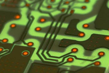
Started early in 2017, the two PCB fabricators Würth Elektronik and FELA with their sites in the land Baden Wurttemberg, have been jointly researching on PCB technology digitization. Prototype results in July were encouraging already – in October both partners dispatched first serial orders of their respective pilot projects.
The s.mask technology pushed by FELA and Würth pursues an approach of coating a defined functional surface by 3-D print, independent of varnish and machine fleet. This is – from both companies‘ perspective – the best starting point for gradually digitizing PCB production and its inherent processes.
Initial material tests and examination results prove a tremendously improved accuracy and various options for an application-specific mask definition. Both offset and basic tolerance ranges can be significantly reduced that way.
Especially the individual surface design allows consideration of customer demands and special requirements, e.g. on dielectric strength values. S.mask as the first and sole technology in the PCB sector allows for direct coating of even more than just one layer of defined and precisely designed dielectric.
First trial series on soldering processes brought another outstanding per-formance to light: Notable improvement could be achieved for most of soldering and assembly issues previously known. Should these observations be confirmed during the test runs envisaged for early 2018, they would yield immense benefits. Both partners are expecting concrete statements for mid of 2018 already.
Norbert Krütt, managing director of FELA in Villingen-Schwenningen, is highly satisfied with the outcomes achieved so far: "The digitization of PCB technology represents a real quantum leap under technological aspects. Functional coatings respectively dielectric are no more generously dispersed like with a watering can but rather utilized in a targeted manner for realizing benefits in downstream processes at both stages, within the PCB production and those at our customers’ sites.“
Beside the advantages in precision and performance, first pilot projects also show an upgrade of the PCB protection, turning out well through gentle application of the functional coating as well as reduced quantity and kind of the chemicals deployed.
The cooperation is conducted at all levels, from top management via R&D up to shared communication. Andreas Gimmer, managing director of Würth Elektronik CBT in Schopfheim, says: "Since the time we started our cooperative partnership, it has been seen that the way our companies are working together provides multifarious synergies. We expect economic success for us, but also find that common research and development is simply pleasure.“
About Würth Elektronik Circuit Board Technology (CBT)
Würth Elektronik Circuit Board Technology was founded in 1971 and has established itself as one of the leading PCB manufacturers in Europe. De-velopers are able get standard circuit boards, new and innovative technolo-gies and even complete system solutions all from one source. Here at Würth Elektronik, we cover the entire product life cycle, from the initial idea for a design, for example during early R&D projects, to the production of prototypes on the online shop WEdirekt and finally, manufacturing of medium and large volumes in Germany or Asia. Knowledgeable specialists are not just located at our German plants. Internationalization is an important strategic aspect for Würth Elektronik. We have numerous sales teams set up across many European countries.
Every day more than 120 new PCB designs enter our production. We have over 4,000 customers, ranging from large corporations to one-man designers. In addition to the personal care provided through our dense network of over 100 internal and external sales people, customers also have the option to purchase printed circuit boards online through the easy to use online shop, WEdirekt.
For more information, click here.
About FELA GmbH
FELA is one of the five largest circuit board manufacturers in Germany and has made the leap from simple contract manufacturer to innovative system provider. “Help us shape the future!” – with this motto, FELA GmbH is a fixture on today’s market.
FELA, a private, independent medium-sized enterprise based in the south-ern Black Forest with a 165-strong workforce, generated sales of €23.6m in 2016. The company has its headquarters in Villingen-Schwenningen and an additional distribution centre in Solingen.
As well as manufacturing and selling FR4-based circuit boards, other mainstays of the company’s activities include manufacturing capacitive glass input systems with the brand name FELAM GLASLINE and, as a technological leader, FELAM THERMOLINE technology, IMS circuit boards and sys-tems for aluminium or copper-based power LED applications. For more information, click here.
Share on:


Testimonial
"Advertising in PCB007 Magazine has been a great way to showcase our bare board testers to the right audience. The I-Connect007 team makes the process smooth and professional. We’re proud to be featured in such a trusted publication."
Klaus Koziol - atgSuggested Items
I-Connect007 Releases The Printed Circuit Designer’s Guide to… Direct Metallization: A Guide to Complex PCB Fabrication
05/13/2026 | I-Connect007As PCB complexity continues to accelerate, fabricators and OEMs are reevaluating long-standing manufacturing processes to meet the demands of AI, HDI, advanced packaging, and next-generation electronics. To address these evolving challenges, I-Connect007 is proud to announce the release of The Printed Circuit Designer’s Guide to… Direct Metallization: A Guide to Complex PCB Fabrication, authored by MacDermid Alpha Solution’s Carmichael Gugliotti.
Driving Innovation: Selecting the Right Laser Source
04/28/2026 | Simon Khesin -- Column: Driving InnovationWhen I first joined Schmoll Maschinen, I brought experience from almost every PCB process, except for laser. As I immersed myself in laser processing, I realized why it can seem so daunting to a newcomer. The complexity arises from three intersecting factors: A vast variety of laser sources: CO2, UV-nano, green-pico, UV-pico, IR-pico, and others; a diverse range of applications: Drilling, cutting, ablation, and more; and an extensive list of materials: These have vastly different absorption rates. Choosing the right machine or laser source is rarely trivial. Even for experienced engineers, answering "Which source is best?" requires examining the business's specific goals.
Institute of Circuit Technology Spring Seminar 2026: A Bright Future in Europe
04/23/2026 | Pete Starkey, I-Connect007Through the leafy lanes and spring flowers of Warwickshire and back to Meridan, the traditional centre of England, and now officially part of the Metropolitan Borough of Solihull in the county of the West Midlands, I attended the Annual General Meeting and Spring Seminar of the Institute of Circuit Technology (ICT) on April 14. Out of the AGM came notable changes in leadership at the top of the Institute: the retirement of Mat Beadel as chair and Emma Hudson as technical director. Effective May 1, Steve Driver is the new chair, and Alun Morgan is the new technical director.
ACCM Unveils Negative and Near-zero CTE Materials for Large-Format AI Chips
04/21/2026 | Advanced Chip and Circuit MaterialsAdvanced Chip and Circuit Materials, Inc. (ACCM) has launched two new materials: Celeritas HM50, with a negative coefficient of thermal expansion (CTE) of -8 ppm/°C to offset the positive CTE and expansion of copper with temperature on circuit boards, and Celeritas HM001, with near-zero CTE and the low-loss performance needed for high-speed signal layers to 224 Gb/s and faster in artificial intelligence (AI) circuits.
Fresh PCB Concepts: Designing PCBs for Harsh Environments—Reliability Is Engineered Upstream
04/23/2026 | Team NCAB -- Column: Fresh PCB ConceptsWhen engineers hear the phrase “harsh environment,” they usually think of the extreme temperature swings, vibration and shock, pressure changes, or radiation in aerospace. However, aerospace is not the only harsh environment where electronic assemblies must survive. Automotive power electronics, downhole oil and gas tools, marine controls, rail systems, defense platforms, and industrial automation equipment all expose PCBs to environments that are equally unforgiving. The stress mechanisms may differ, but the physics does not.