


 Trouble in Your Tank: Organic Addition Agents in Electrolytic Copper Plating
 It’s Only Common Sense: Selling During an Economic Downturn
 Marcy’s Musings: Can You Hear the Voices?


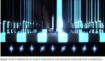
Complete Design of a Silicon Quantum Computer Chip Unveiled
December 15, 2017 | UNSWEstimated reading time: 7 minutes
Research teams all over the world are exploring different ways to design a working computing chip that can integrate quantum interactions. Now, UNSW engineers believe they have cracked the problem, reimagining the silicon microprocessors we know to create a complete design for a quantum computer chip that can be manufactured using mostly standard industry processes and components.
The new chip design, published in the journal Nature Communications, details a novel architecture that allows quantum calculations to be performed using existing semiconductor components, known as CMOS (complementary metal-oxide-semiconductor) - the basis for all modern chips.
It was devised by Andrew Dzurak, director of the Australian National Fabrication Facility at the University of New South Wales (UNSW), and Dr Menno Veldhorst, lead author of the paper who was a research fellow at UNSW when the conceptual work was done.
"We often think of landing on the Moon as humanity's greatest technological marvel," said Dzurak, who is also a Program Leader at Australia's famed Centre of Excellence for Quantum Computation and Communication Technology (CQC2T). "But creating a microprocessor chip with a billion operating devices integrated together to work like a symphony - that you can carry in your pocket! - is an astounding technical achievement, and one that's revolutionised modern life.
"With quantum computing, we are on the verge of another technological leap that could be as deep and transformative. But a complete engineering design to realise this on a single chip has been elusive. I think what we have developed at UNSW now makes that possible. And most importantly, it can be made in a modern semiconductor manufacturing plant," he added.
Veldhorst, now a team leader in quantum technology at QuTech - a collaboration between Delft University of Technology and TNO, the Netherlands Organisation for Applied Scientific Research - said the power of the new design is that, for the first time, it charts a conceivable engineering pathway toward creating millions of quantum bits, or qubits.
"Remarkable as they are, today's computer chips cannot harness the quantum effects needed to solve the really important problems that quantum computers will. To solve problems that address major global challenges - like climate change or complex diseases like cancer - it's generally accepted we will need millions of qubits working in tandem. To do that, we will need to pack qubits together and integrate them, like we do with modern microprocessor chips. That's what this new design aims to achieve.
"Our design incorporates conventional silicon transistor switches to 'turn on' operations between qubits in a vast two-dimensional array, using a grid-based 'word' and 'bit' select protocol similar to that used to select bits in a conventional computer memory chip," he added. "By selecting electrodes above a qubit, we can control a qubit's spin, which stores the quantum binary code of a 0 or 1. And by selecting electrodes between the qubits, two-qubit logic interactions, or calculations, can be performed between qubits."
A quantum computer exponentially expands the vocabulary of binary code used in modern computers by using two spooky principles of quantum physics - namely, 'entanglement' and 'superposition'. Qubits can store a 0, a 1, or an arbitrary combination of 0 and 1 at the same time. And just as a quantum computer can store multiple values at once, so it can process them simultaneously, doing multiple operations at once.
This would allow a universal quantum computer to be millions of times faster than any conventional computer when solving a range of important problems.
But to solve complex problems, a useful universal quantum computer will need a large number of qubits, possibly millions, because all types of qubits we know are fragile, and even tiny errors can be quickly amplified into wrong answers.
"So we need to use error-correcting codes which employ multiple qubits to store a single piece of data," said Dzurak. "Our chip blueprint incorporates a new type of error-correcting code designed specifically for spin qubits, and involves a sophisticated protocol of operations across the millions of qubits. It's the first attempt to integrate into a single chip all of the conventional silicon circuitry needed to control and read the millions of qubits needed for quantum computing."
"We expect that there will still be modifications required to this design as we move towards manufacture, but all of the key components that are needed for quantum computing are here in one chip. And that's what will be needed if we are to make quantum computers a workhorse for calculations that are well beyond today's computers," Dzurak added. "It shows how to integrate the millions of qubits needed to realise the true promise of quantum computing."
Building such a universal quantum computer has been called the 'space race of the 21st century'. For a range of calculations, they will be much faster than existing computers, and for some challenging problems they could find solutions in days, maybe even hours, when today's best supercomputers would take millions of years.
Page 1 of 2
Share on:


Suggested Items
Explore Thermal Management Solutions in Latest Podcast Series—New Episode Now Available
04/23/2025 | I-Connect007I-Connect007 is excited to share the latest episode in our new podcast series! In this episode, Ryan returns to discuss practical strategies for managing heat, starting early in the design planning and specification phases. After all, prevention means there’s less to mitigate later.
Learning to Speak ‘Fab’
04/23/2025 | Ray Fugitt, DownStream TechnologiesOver the years, I’ve seen many PCB designers make DFM mistakes. At DownStream, I work with design and fabrication, and sometimes it feels as if the two segments are speaking completely different languages. But once designers learn to speak “fab,” many of these DFM challenges disappear.
Flex Wins Two 2025 PACE Awards for Innovation in Automotive Compute and Power Electronics
04/22/2025 | PRNewswireFlex was named a two-time 2025 Automotive News PACE Award winner at the awards ceremony on April 15, recognized for its industry-leading Jupiter Compute Platform and Backup DC/DC Converter design platforms.
Material Selection and RF Design
04/21/2025 | Andy Shaughnessy, Design007 MagazineInnovation rarely sleeps in this industry, and the RF laminate segment offers a perfect example. RF materials have continued to evolve, providing PCB designers much more than an either/or choice. I asked materials expert Alun Morgan, technology ambassador for the Ventec International Group, to walk us through the available RF material sets and how smart material selection can ease the burden on RF designers and design engineers.
Real Time with... IPC APEX EXPO 2025: Aster—Enhancing Design for Effective Testing Strategies
04/18/2025 | Real Time with...IPC APEX EXPOWill Webb, technical director at Aster, stresses the importance of testability in design, emphasizing early engagement to identify testing issues. This discussion covers the integration of testing with Industry 4.0, the need for good test coverage, and adherence to industry standards. Innovations like boundary scan testing and new tools for cluster testing are introduced, highlighting advancements in optimizing testing workflows and collaboration with other tools.