


 Marcy’s Musings: Operating Without a Rulebook
 It’s Only Common Sense: Hire for Hunger, Train for Skill
 Dan’s Biz Bookshelf: ‘The 'NVIDIA Way: Jensen Huang and the Making of a Tech Giant’


Hitachi Chemical to Build New Factory in Taiwan to Manufacture Laminate Materials for PWB
April 18, 2018 | Hitachi Chemical Co., Ltd.Estimated reading time: Less than a minute
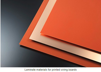
Hitachi Chemical Co., Ltd. has decided to construct a new factory to manufacture advanced functional laminate materials for printed wiring boards (pre-preg and copper-clad laminates) on the site of Hitachi Chemical Electronic Materials (Taiwan) Co., Ltd. (HCET), Hitachi Chemical's subsidiary in Taiwan. Hitachi Chemical will invest a total of approximately 7.5 billion yen and the new factory will begin operation by April 2020.
Hitachi Chemical's laminate materials for printed wiring boards are being well received in the market, especially with demand for its advanced functional laminate materials for semiconductor packaging substrates used in various fields, including 5th generation wireless systems (5G), advanced driver-assistance systems (ADAS) and artificial intelligence (AI), expected to grow stronger in the medium- to long-term. To address its customer needs promptly under these circumstances, Hitachi Chemical has decided to invest in establishing a supply system in Taiwan, the biggest demand center for advanced functional laminate materials.
Hitachi Chemical will take advantage of this new factory to boost the sales of its advanced functional laminate materials by developing a production system capable of delivering timely supplies to its customers.
Share on:


Testimonial
"Your magazines are a great platform for people to exchange knowledge. Thank you for the work that you do."
Simon Khesin - Schmoll MaschinenSuggested Items
Nortech Systems Launches Power over Fiber Technology Platform for EMI-Sensitive Applications
04/08/2026 | Globe NewswireNortech Systems Incorporated, a leading provider of design and manufacturing solutions for complex electromedical devices and electromechanical systems, has announced the launch of its Power over Fiber technology platform.
Flexible Thinking: Designing Flex Circuits for Dynamic Reliability
04/09/2026 | Joe Fjelstad -- Column: Flexible ThinkingFlex circuits flex. No surprises there. However, they are also very commonly designed into products because they are thin and offer consistent thickness and dielectric properties, attributes highly prized by present-day product designers of personal electronics. This would include smartphones and, increasingly, wearable electronics for medical monitoring and even fashion.
Understanding Tolerances in Flexible Circuit Design
04/01/2026 | Chris Clark, Flexible Circuit TechnologiesThe challenge with cumulative tolerances is meeting the dimensional requirements for items dimensioned on a drawing or specification for a flexible or rigid-flex circuit. It is critical to understand the fabrication processes and how features are defined when creating your tolerance requirements.
Target Condition: An Exploration of Flooding PCB Layers
04/02/2026 | Kelly Dack -- Column: Target ConditionThe concept of flooding PCB layers with copper has been around for so long, you’d think we’d have it mastered. We haven’t. (Oh, and by “we,” I mean design engineers and the software tools we depend on.) Years ago, PCB artwork was created by hand using light tables, with tape applied to Mylar. Signals were slow, traces were relatively wide, and high-current paths were simply “beefed up” with wider copper. Signal integrity wasn’t yet a driving concern. Today, solid return paths are fundamental to robust design. We understand the importance of continuous reference planes for signal integrity and EMI control.
New, Greener Solutions for Etch: Novel Copper Extraction
03/30/2026 | Richard Nichols, GreenSource Engineering“Novel” is a typical marketing phrase that implies new and unique, but often “novel” actually means an established technology being applied to a new field or application. This, in turn, is often driven by newly relevant external motivation. GreenSource has been working on just such a solution: novel copper extraction, offering a better and greener alternative to traditional LLE control systems for cupric chloride etch.