


 Global Citizenship: Together for a Perfect PCB Solution
 Smart Automation: Odd-form Assembly—Dedicated Insertion Equipment Matters
 Nolan’s Notes: Everyone Has Their Eye on India


SemiGen Strengthens PCB Assembly, Test Capabilities
September 18, 2018 | SemiGenEstimated reading time: 2 minutes
After moving into their new state-of-the- art facility, SemiGen Inc., an ISO and ITAR registered outsource for RF and microwave contract assembly, automated PCB assembly (PCBA), wafer-processing, and key diodes, semiconductor devices, and bonding supplies, has made an additional capital investment of over a half million dollars in new production, wafer fab, and testing equipment to support customer demand.
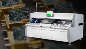
The new equipment consists of improvements across their entire service platform and includes a new Mycronic MY300 pick-and-place system; two new Westbond wire bonders, a new Centrotherm eutectic vacuum chamber, new HTOL / HTRB ovens; as well as a new Disco DAD3220 dicing saw. In addition, they’ve made upgrades in their high-frequency testing department which includes several new pieces of performance testing and metrology tools.
"I'm excited to be in a position to continue to invest in and grow this important domestic outsource business," said Tim Filteau, president of SemiGen. "Our CEO, Jim Morgan, has said we must do our best to help our customers augment their design, assembly, and hi-rel testing and up-screening capabilities, and it feels great to see this new equipment getting up and running to do just that."
SemiGen is a USA-based outsource to OEMs in the RF/microwave, military, space, homeland security, optical, medical device, and commercial wireless markets. Their services and products are designed to fill voids in the manufacturing supply chain and production floor. SemiGen’s design and manufacturing center includes wire bonding to Si, GaAs, and GaN chips, RF/microwave and PCB assembly, mixed signal digital and analog assembly, module repair, and high frequency testing and upscreening services. In recent years, SemiGen has invested in coupling their services with in-stock product solutions by carrying the diodes, active and passive semiconductor devices, and bonding supplies needed for successful production of several types of solid-state, multi-function assemblies (MFAs) and components.
Their team helps with designs, builds prototypes, and handles volume production runs within new their 37,000 square foot facility in Manchester, New Hampshire. The facility also includes a class 10,000 clean room. Manual to fully automatic assembly solutions are now available.
With their recent upgrades in place, SemiGen is also offering wafer processing of silicon wafers, as well as processing ceramic substrates. Processing services provided include any combination of photolithography, wet etch, dry etch, metallization, grinding, polishing, and in-process metrology.
Their recent investments in their RF and Microwave testing and environmental screening lab has also enabled them to offer high-reliability (Hi-rel) screening of amplifiers, FETs, MMICs, transistors, diodes, and other RF and microwave components operating up into millimeter-wave frequencies.
Tests can be performed and delivered with full documentation in adherence with MIL-PRF-19500, MILPRF-38534, and MIL-PRF-38535 requirements. Element evaluation and screening options from Class H, Class K, TX, TXV, S-level, as well as custom SCD driven requirements, are available.
Share on:


Testimonial
"In a year when every marketing dollar mattered, I chose to keep I-Connect007 in our 2025 plan. Their commitment to high-quality, insightful content aligns with Koh Young’s values and helps readers navigate a changing industry. "
Brent Fischthal - Koh YoungSuggested Items
Variosystems Strengthens North American Presence with Southlake Relaunch 2025
09/15/2025 | VariosystemsVariosystems celebrated the relaunch of its U.S. facility in Southlake, Texas. After months of redesign and reorganization, the opening marked more than just the return to a modernized production site—it was a moment to reconnect with our teams, partners, and the local community.
MacDermid Alpha Presents at SMTA New Delhi, Bangalore Chapter, on Flux–OSP Interaction
09/09/2025 | MacDermid Alpha Electronics SolutionsMacDermid Alpha contributes technical insights on OSP solderability at the Bangalore Chapter, SMTA reinforcing commitment to knowledge-sharing and industry collaboration.
Naprotek Appoints Mark Crebs to Lead Business Development for Products and Platforms
08/27/2025 | Naprotek LLCNaprotek, LLC, a leading provider of mission-critical electronics technology solutions, announced the appointment of Mark Crebs to Products and Platform Director of Business Development.
VVDN Expands Manufacturing Footprint into the UAE to Meet Global Demand
08/20/2025 | PRNewswireVVDN Technologies, a global provider of software, product engineering and electronics manufacturing services & solutions, today announced it is setting up a new manufacturing facility in the UAE as part of its global expansion strategy.
SisTech Manufacturing Expands Services: Leading Precision in Electronic Manufacturing
08/11/2025 | Globe NewswireSisTech Manufacturing, known for its expertise in precision electronic manufacturing services, is expanding what it can do in production. For over 30 years, the company has been recognized for its commitment to quality and its ability to meet the diverse demands of industries like aerospace and consumer electronics. With ISO 9001:2015 certification and ITAR registration,