


 It’s Only Common Sense: Selling to Today's Generation of Buyers
 Dan’s Biz Bookshelf: ‘Believe in Better'
 The Big Picture: Our Big ‘Why’ in the Age of AI


To Guide Cancer Therapy, Device Quickly Tests Drugs on Tumor Tissue
December 12, 2018 | MITEstimated reading time: 6 minutes
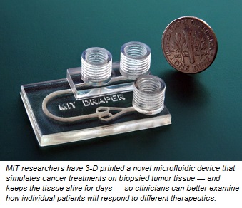
MIT researchers have 3-D printed a novel microfluidic device that simulates cancer treatments on biopsied tumor tissue, so clinicians can better examine how individual patients will respond to different therapeutics—before administering a single dose.
Testing cancer treatments today relies mostly on trial and error; patients may undergo multiple time-consuming and hard-to-tolerate therapies in pursuit of one that works. Recent innovations in pharmaceutical development involve growing artificial tumors to test drugs on specific cancer types. But these models take weeks to grow and don’t account for an individual patient’s biological makeup, which can affect treatment efficacy.
The researchers’ device, which can be printed in about one hour, is a chip slightly larger than a quarter, with three cylindrical “chimneys” rising from the surface. These are ports used to input and drain fluids, as well as remove unwanted air bubbles. Biopsied tumor fragments are placed in a chamber connected to a network of channels that deliver fluids—containing, for instance, immunotherapy agents or immune cells—to the tissue. Clinicians can then use various imaging techniques to see how the tissue responds to the drugs.
A key feature was using a new biocompatible resin—traditionally used for dental applications—that can support long-term survival of biopsied tissue. Although previous 3-D-printed microfluidics have held promise for drug testing, chemicals in their resin usually kill cells quickly. The researchers captured fluorescence microscopy images that show their device, called a tumor analysis platform (TAP), kept more than 90% of the tumor tissue alive for at least 72 hours, and potentially much longer.
Because the 3-D printed device is easy and cheap to fabricate, it could be rapidly implemented into clinical settings, the researchers say. Doctors could, for instance, print out a multiplexed device that could support multiple tumor samples in parallel, to enable modeling of the interactions between tumor fragments and many different drugs, simultaneously, for a single patient.
“People anywhere in the world could print our design. You can envision a future where your doctor will have a 3-D printer and can print out the devices as needed,” says Luis Fernando Velásquez-García, a researcher in the Microsystems Technology Laboratories and co-author on a paper describing the device, which appears in the December issue of the Journal of Microelectromechanical Systems. “If someone has cancer, you can take a bit of tissue in our device, and keep the tumor alive, to run multiple tests in parallel and figure out what would work best with the patient’s biological makeup. And then implement that treatment in the patient.”
A promising application is testing immunotherapy, a new treatment method using certain drugs to rev up a patient’s immune system to help it fight cancer. (This year’s Nobel Prize in physiology or medicine was awarded to two immunotherapy researchers who designed drugs that block certain proteins from preventing the immune system from attacking cancer cells.) The researchers’ device could help doctors better identify treatments to which an individual is likely to respond.
“Immunotherapy treatments have been specifically developed to target molecular markers found on the surface of cancer cells. This helps to ensure that the treatment elicits an attack on the cancer directly while limiting negative impacts on healthy tissue. However, every individual’s cancer expresses a unique array of surface molecules—as such, it can be difficult to predict who will respond to which treatment. Our device uses the actual tissue of the person, so is a perfect fit for immunotherapy,” says first author Ashley Beckwith SM ’18, a graduate researcher in Velásquez-García’s research group.
Co-author on the paper is Jeffrey T. Borenstein, a researcher at Draper.
Page 1 of 2
Share on:


Suggested Items
United Electronics Corporation Advances Manufacturing Capabilities with Schmoll MDI-ST Imaging Equipment
06/24/2025 | United Electronics CorporationUnited Electronics Corporation has successfully installed the advanced Schmoll MDI-ST (XL) imaging equipment at their advanced printed circuit board facility. This significant technology investment represents a continued commitment to delivering superior products and maintaining their position as an industry leader in precision PCB manufacturing.
Orbel Corporation Integrates Schmoll Direct Imaging
06/04/2025 | Schmoll AmericaOrbel Corporation in Easton, PA, proudly becomes the first PCM facility in the U.S. equipped with Schmoll’s MDI Direct Imaging system. This installation empowers Orbel to support customers with greater precision and quality.
Key Insights on Photoresist for Defect Reduction
05/21/2025 | I-Connect007 Editorial TeamIn PCB manufacturing, understanding the intricacies of the photoresist process is crucial for achieving high-quality results. Industry experts Josh Krick, a technical service engineer at IEC, and Tim Blair, a PCB imaging specialist at Tim Blair LLC, share their knowledge on the essential stages of photoresist application, highlight critical advancements in materials, and discuss common defects encountered during production. They share best practices and innovative solutions to enhance the manufacturing process, reduce defects, and ensure efficiency and reliability in high-tech applications.
NXP Unveils Third-Generation Imaging Radar Processors for Level 2+ to 4 Autonomous Driving
05/09/2025 | NXP SemiconductorNXP Semiconductors N.V. unveiled its new S32R47 imaging radar processors in 16 nm FinFET technology, building on NXP’s proven expertise in the imaging radar space.
SEMICON Europa 2025 Call for Abstracts Opens for Advanced Packaging Conference and MEMS & Imaging Summit
05/05/2025 | SEMISEMI Europe announced the opening of the call for abstracts for SEMICON Europa 2025, to be held November 18-21 at Messe München in Munich, Germany. Selected speakers will share their expertise at the Advanced Packaging Conference (APC), MEMS & Imaging Sensors Summit, and during presentations on the show floor.