


 Dan’s Biz Bookshelf: ‘The Next RenAIssance: AI and the Expansion of Human Potential’
 The Chemical Connection: When the Industry Moves Faster Than the Standards
 Driving Innovation: Selecting the Right Laser Source


Using Big Databases to Find Superconductors of the Future
January 14, 2019 | ACN NewswireEstimated reading time: 2 minutes
Japanese researchers have found an approach to more quickly and successfully identify superconducting materials.
"The data-driven approach shows promising power to accelerate the discovery of new thermoelectric and superconducting materials," the researchers say in their study published in the journal Science and Technology of Advanced Materials.
Superconductors are materials that conduct electricity with virtually no resistance. Superconducting materials have improved the field of magnetic resonance imaging (MRI) and have led to the development of particle colliders that can be used for research related to splitting atoms. Currently available superconducting materials can only perform at extremely low temperatures. If researchers can find superconducting materials that work at ambient temperature, electricity could be conducted over large distances without energy loss.
Current approaches to searching for these materials are somewhat random, and results strongly depend on researcher's intuition, experience and luck. Materials scientist Yoshihiko Takano of Japan's National Institute for Materials Science and colleagues have shown that sifting through an inorganic materials database using specific search parameters can provide a more systematic way to finding superconducting materials.
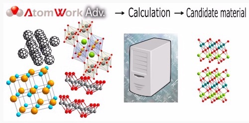
They searched through AtomWork, a large database for inorganic materials. In a previous study using this same approach, the team identified SnBi2Se4 (a compound of tin, bismuth, and selenium) as a potential superconductor. Experiments showed that this was indeed the case.
But SnBi2Se4 requires very low temperatures and high pressures to become superconductive. The team searched once more through the database, selecting materials that have a similar crystal structure to SnBi2Se4 but a narrower 'band gap', a property related to atomic structure that allows electrons to jump up from one energy level to another and thus partake in electrical conductivity.
Their best choice was PbBi2Te4 (formed of lead, bismuth, and tellurium). They synthesised PbBi2Te4 crystals, examined their structure, chemical composition and other properties, and found that those properties met the predictions. They exposed the crystals to high pressures and varying temperatures and found that the electrical resistance of PbBi2Te4 decreased with increasing pressure, reaching a superconductive state at 10 gigapascals, about half the pressure needed for SnBi2Se4 to become superconductive.
This work "presents a case study for the important first-step for the next-generation data-driven materials science," the team concludes.
About Science and Technology of Advanced Materials (STAM) Journal
Open access journal, STAM publishes outstanding research articles across all aspects of materials science, including functional and structural materials, theoretical analyses, and properties of materials.
Share on:


Subscribe
Stay ahead of the technologies shaping the future of electronics with our latest newsletter, Advanced Electronics Packaging Digest. Get expert insights on advanced packaging, materials, and system-level innovation, delivered straight to your inbox.Subscribe now to stay informed, competitive, and connected.
Suggested Items
From Backbone to Breakthroughs: I-Connect007 Wraps PCB Materials Series with Focus on Innovation
04/30/2026 | I-Connect007I-Connect007 wraps up its six-part podcast series, PCB Materials: The Backbone and Future of Electronics, with Episode 6 and a discussion focusing on innovation. In Episode 6, Marcy LaRont speaks with Isola CTO Kirk Thompson about a critical turning point for the PCB industry as innovation accelerates. As data rates climb and demands from AI infrastructure, power density, flexible electronics, photonics, and chiplet integration intensify, traditional material assumptions are no longer sufficient.
Jiva Soluboard Getting the Attention It Deserves
04/30/2026 | Marcy LaRont, I-Connect007 MagazineJiva is a newer company that bridges the divide between PCB fabrication and product circularity or sustainability. Jiva Soluboard is the first fully recyclable laminate material ever created for PCB fabrication, and it's not going unnoticed. Stephen Driver, CEO of Jiva, gave us an update at APEX EXPO, including an exciting certification achievement in February.
Driving Innovation: Selecting the Right Laser Source
04/28/2026 | Simon Khesin -- Column: Driving InnovationWhen I first joined Schmoll Maschinen, I brought experience from almost every PCB process, except for laser. As I immersed myself in laser processing, I realized why it can seem so daunting to a newcomer. The complexity arises from three intersecting factors: A vast variety of laser sources: CO2, UV-nano, green-pico, UV-pico, IR-pico, and others; a diverse range of applications: Drilling, cutting, ablation, and more; and an extensive list of materials: These have vastly different absorption rates. Choosing the right machine or laser source is rarely trivial. Even for experienced engineers, answering "Which source is best?" requires examining the business's specific goals.
Insulectro: Advanced PCB Fabrication Materials
04/23/2026 | Real Time with... APEX EXPOExplore advanced PCB fabrication materials with Insulectro's Dain Hertsgaard and Gabriel Zepeda. This interview covers Arlon's innovative polyimide and epoxy solutions, including low-flow options for flex materials and high-performance materials for HDI applications; Qnity's polyimide films for demanding environments, and DuPont Interra's capacitance films for enhanced reliability. Insulectro offers comprehensive service and a commitment to advancing circuit technology
A Mic, a Tiny Cam, and the Show Floor: The Story Behind 'Take the Mic!'
04/23/2026 | I-Connect007 Editorial TeamI-Connect007’s Take the Mic! program at APEX EXPO 2026 in Anaheim is proving to be a must-watch feature for this year’s event coverage, as we invited company representatives to participate in a sponsored conversation about their businesses and products in a whole new way: in front of a camera at their booths. While our managing editors and guest editors were conducting slightly longer Real Time with… APEX EXPO interviews in our booth, three staff members and guests acted as roaming reporters, conducting short, prearranged interviews with several companies exhibiting on the show floor.