


 Driving Innovation: Selecting the Right Laser Source
 Dan’s Biz Bookshelf: ‘Notorious: Leadership Lessons From History’s Most Notorious Leaders’ (New Audio Version)
 It's Only Common Sense: See Your Marketing as a Discipline, Not a Department


Scientists Boost Stability of Low-Cost, Large-Area Solar Modules
January 23, 2019 | OISTEstimated reading time: 3 minutes
Scientists at the Okinawa Institute of Science and Technology Graduate University (OIST) have resolved a fundamental weakness in a promising solar technology known as Perovskite Solar Cells, or PSCs. Their innovations appear to improve both the devices’ stability and scalability in one fell swoop and could be key to moving PSCs to market.
Third-generation solar cells efficiently convert sunlight into usable electricity and cost less energy to manufacture than old-school silicon cells. PSCs, in particular, have garnered the attention of science and industry thanks to their low cost and high efficiency. Though their performance is promising in lab tests, the devices still suffer from low stability and cannot be produced commercially until they’re built to last.
“We need solar modules that can last for at least 5 to 10 years. For now, the lifetime of PSCs is much shorter,” said Dr. Longbin Qiu, first author of the paper and a postdoctoral scholar in the OIST Energy Materials and Surface Sciences Unit, led by Prof. Yabing Qi.
The study, published online in Advanced Functional Materials on December 13, 2018, supports prior evidence that a commonly used material in PSCs, called titanium dioxide, degrades the devices and limits their lifetime. The researchers replaced this material with tin dioxide, a stronger conductor without these degrading properties. They optimized their method of applying tin dioxide to produce stable, efficient and scalable PSCs.
In experiments, the researchers found that tin dioxide-based devices showed lifetimes over three times longer than PSC devices using titanium dioxide. “Tin dioxide can give users the device performance they need,” said Qiu.
An Improved Design
PSCs consist of layered materials, each with a specific function. The “active layer,” made from perovskite materials, absorbs incoming sunlight in the form of particles called photons. When a photon strikes a solar cell, it generates negatively-charged electrons and positively-charged holes in the active layer. Scientists control the flow of these electrons and holes by sandwiching the active layer between two “transport materials,” thus creating a built-in electrical field.
To help usher electrons in the right direction, many PSCs include an “electron transport layer.” Most PSCs employ titanium dioxide as their electron transport layer, but when exposed to sunlight, the material reacts with perovskite and ultimately degrades the device. Tin dioxide stands as a viable replacement for titanium dioxide, but before this study, it had not been successfully incorporated into a large-scale device.
Using a common technique in the industry called sputtering deposition, the researchers learned how to craft an effective electron transport layer from tin dioxide. Sputtering deposition works by bombarding the target material, here tin dioxide, with charged particles, causing it to spray upwards onto a waiting surface. By precisely controlling the power of the sputtering and speed of the deposition, the researchers produced smooth layers with a uniform thickness over a large area.
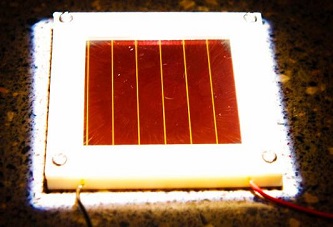
*Their new solar cells achieved an efficiency of over 20%. To demonstrate the scalability of this new method, the researchers then fabricated 5 by 5 centimeter solar modules with a designated area of 22.8 square-centimeters, finding that the resulting devices showed over 12% efficiency. This research, which was supported by the OIST Technology Development and Innovation Center’s Proof-of-Concept Program, represents a crucial step forward towards meeting the current industry standard for PSC efficiency.
Dr. Longbin Qiu holds up a sheet of solar cells made from flexible materials. The Energy Materials and Surface Sciences Unit aims to develop these devices to craft solar curtains and solar technologies that can be easily incorporated into people’s homes.
Moving to Market
The researchers plan to continue optimizing their PSC design with the goal of producing large-scale solar modules with improved efficiency. The research unit experiments with flexible, transparent solar devices and aims to apply their optimized PSC design in solar windows, curtains, backpacks and deployable charging units.
“We want to scale these devices up to a large size, and though their efficiency is already reasonable, we want to push it further,” said Prof. Qi. “We are optimistic that in the next few years, this technology will be viable for commercialization.”
Share on:


Subscribe
Stay ahead of the technologies shaping the future of electronics with our latest newsletter, Advanced Electronics Packaging Digest. Get expert insights on advanced packaging, materials, and system-level innovation, delivered straight to your inbox.Subscribe now to stay informed, competitive, and connected.
Suggested Items
Driving Innovation: Selecting the Right Laser Source
04/28/2026 | Simon Khesin -- Column: Driving InnovationWhen I first joined Schmoll Maschinen, I brought experience from almost every PCB process, except for laser. As I immersed myself in laser processing, I realized why it can seem so daunting to a newcomer. The complexity arises from three intersecting factors: A vast variety of laser sources: CO2, UV-nano, green-pico, UV-pico, IR-pico, and others; a diverse range of applications: Drilling, cutting, ablation, and more; and an extensive list of materials: These have vastly different absorption rates. Choosing the right machine or laser source is rarely trivial. Even for experienced engineers, answering "Which source is best?" requires examining the business's specific goals.
Insulectro: Advanced PCB Fabrication Materials
04/23/2026 | Real Time with... APEX EXPOExplore advanced PCB fabrication materials with Insulectro's Dain Hertsgaard and Gabriel Zepeda. This interview covers Arlon's innovative polyimide and epoxy solutions, including low-flow options for flex materials and high-performance materials for HDI applications; Qnity's polyimide films for demanding environments, and DuPont Interra's capacitance films for enhanced reliability. Insulectro offers comprehensive service and a commitment to advancing circuit technology
A Mic, a Tiny Cam, and the Show Floor: The Story Behind 'Take the Mic!'
04/23/2026 | I-Connect007 Editorial TeamI-Connect007’s Take the Mic! program at APEX EXPO 2026 in Anaheim is proving to be a must-watch feature for this year’s event coverage, as we invited company representatives to participate in a sponsored conversation about their businesses and products in a whole new way: in front of a camera at their booths. While our managing editors and guest editors were conducting slightly longer Real Time with… APEX EXPO interviews in our booth, three staff members and guests acted as roaming reporters, conducting short, prearranged interviews with several companies exhibiting on the show floor.
Target Condition: When Design Outpaces Manufacturing
04/23/2026 | Kelly Dack -- Column: Target ConditionMost PCB designers already understand why design for manufacturing (DFM) matters. If a product can’t be built reliably, repeatedly, and at a price anyone will actually pay, it’s dead on arrival. You may have the most elegant schematic and layout ever drawn in a CAD tool, but if the PCB suppliers can’t make it, or the EMS sources refuse to quote it, you may well be considered more of a Nutty Professor or well-meaning inventor than a PCB designer.
AGC's Advanced PCB Material Solutions
04/17/2026 | Real Time with... APEX EXPOAGC's line includes advanced PCB materials for critical industries such as aerospace, defense, and medical. This interview highlights their commitment to North American sourcing, offering solutions to today's challenges. AGC provides specialized automotive PCB materials including fastRise, a low-loss non-reinforced prepreg designed for high-frequency applications like 77 GHz radar.