


 Dan's Biz Bookshelf: 'Move Your Bus'
 Driving Innovation: Direct Imaging vs. Conventional Exposure
 It’s Only Common Sense: Selling to Today's Generation of Buyers


Laser Processing Method to Increase Efficiency of Optoelectronic Devices
April 15, 2019 | NRLEstimated reading time: 2 minutes
Scientists at the U.S. Naval Research Laboratory (NRL) discovered a new method to passivate defects in next generation optical materials to improve optical quality and enable the miniaturization of light emitting diodes and other optical elements.
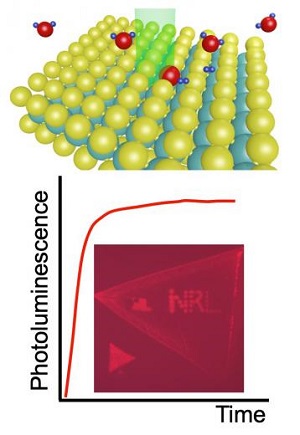
Image Caption: (Top) Illustration of a water molecule bonding at a sulfur vacancy in the MoS2 upon laser light exposure. (Bottom) Photoluminescence (PL) increase observed during laser light exposure in ambient. (Inset) Fluorescence image showing brightened regions spelling out “NRL.” (U.S. Naval Research Laboratory)
“From a chemistry standpoint, we have discovered a new photocatalytic reaction using laser light and water molecules, which is new and exciting,” said Saujan Sivaram, Ph.D., lead author of the study. “From a general perspective, this work enables the integration of high quality, optically active, atomically thin material in a variety of applications, such as electronics, electro-catalysts, memory, and quantum computing applications.”
The NRL scientists developed a versatile laser processing technique to significantly improve the optical properties of monolayer molybdenum disulphide (MoS2)—a direct gap semiconductor—with high spatial resolution. Their process produces a 100-fold increase in the material’s optical emission efficiency in the areas “written” with the laser beam.
According to Sivaram, atomically thin layers of transition metal dichalcogenides (TMDs), such as MoS2, are promising components for flexible devices, solar cells, and optoelectronic sensors due to their high optical absorption and direct band gap.
“These semiconducting materials are particularly advantageous in applications where weight and flexibility are a premium,” he said. “Unfortunately, their optical properties are often highly variable and non-uniform making it critical to improve and control the optical properties of these TMD materials to realize reliable high efficiency devices.”
“Defects are often detrimental to the ability of these monolayer semiconductors to emit light,” Sivaram said. “These defects act as non-radiative trap states, producing heat instead of light, therefore, removing or passivating these defects is an important step towards high efficiency optoelectronic devices.”
In a traditional LED, approximately 90% of the device is a heat sink to improve cooling. Reduced defects enable smaller devices to consume less power, which results in a longer operational lifetime for distributed sensors and low-power electronics.
The researchers demonstrated that water molecules passivate the MoS2 only when exposed to laser light with an energy above the band gap of the TMD. The result is an increase in photoluminescence with no spectral shift.
Treated regions maintain a strong light emission compared to the untreated regions that exhibit much a weaker emission. This suggest that the laser light drives a chemical reaction between the ambient gas molecules and the MoS2.
“This is a remarkable achievement,” said Berend Jonker, Ph.D., senior scientist and principal investigator. “The results of this study pave the way for the use of TMD materials critical to the success of optoelectronic devices and relevant to the Department of Defense mission.”
Share on:


Suggested Items
Symposium Review: Qnity, DuPont, and Insulectro Forge Ahead with Advanced Materials
07/02/2025 | Barb Hockaday, I-Connect007In a dynamic and informative Innovation Symposium hosted live and on Zoom on June 25, 2025, representatives from Qnity (formerly DuPont Electronics), DuPont, and Insulectro discussed the evolving landscape of flexible circuit materials. From strategic corporate changes to cutting-edge polymer films, the session offered deep insight into design challenges, reliability, and next-gen solutions shaping the electronics industry.
Indium Corporation Expert to Present on Automotive and Industrial Solder Bonding Solutions at Global Electronics Association Workshop
06/26/2025 | IndiumIndium Corporation Principal Engineer, Advanced Materials, Andy Mackie, Ph.D., MSc, will deliver a technical presentation on innovative solder bonding solutions for automotive and industrial applications at the Global Electronics A
Gorilla Circuits Elevates PCB Precision with Schmoll’s Optiflex II Alignment System
06/23/2025 | Schmoll MaschinenGorilla Circuits, a leading PCB manufacturer based in Silicon Valley, has enhanced its production capabilities with the addition of Schmoll Maschinen’s Optiflex II Post-Etch Punch system—bringing a new level of precision to multilayer board fabrication.
Day 1: Cutting Edge Insights at the EIPC Summer Conference
06/17/2025 | Pete Starkey, I-Connect007The European Institute for the PCB Community (EIPC) Summer Conference took place this year in Edinburgh, Scotland, June 3-4. This is the second of three articles on the conference. The other two cover the keynote speeches and Day 2 of the technical conference. Below is a recap of the first day’s sessions.
American Made Advocacy: Supporting the Entire PCB Ecosystem—Materials to OEMs
06/17/2025 | Shane Whiteside -- Column: American Made AdvocacyWith the addition of RTX to PCBAA’s membership roster, we now represent the interests of companies in the entire PCB ecosystem. From material providers to OEMs, the insights of our collective members help us educate, advocate, and support legislation and policy favorable to America’s microelectronics manufacturers. The industry veterans who lead these companies provide valuable perspective, and their accumulated wisdom makes us an even stronger association.