


 Driving Innovation: Mechanical and Optical Processes During Rigid-flex Production
 It’s Only Common Sense: Your Biggest Competitor Is Complacency
 The Chemical Connection: Onshoring PCB Production—Daunting but Certainly Possible


Taiyo America Opens San Jose, California Office
June 12, 2019 | Taiyo AmericaEstimated reading time: 1 minute
Taiyo America Inc., a subsidiary of Taiyo Holdings Co. Ltd, has opened a new office in Silicon Valley, USA.
As the advancement of electronics such as IoT technology and the development of AI accelerates, Taiyo's business domain has also changed dramatically across a wide range to now include electronics, energy, agriculture and pharmaceuticals.
In response to these shifts, Taiyo has opened an office in Silicon Valley where the leading-edge electronics technologies are integrated. At the Silicon Valley office, Taiyo will build and strengthen networks and partner relationships with global technology companies. By investing in our relationships with companies that develop innovative technologies and business models, Taiyo will expand current business, and create new business opportunities.
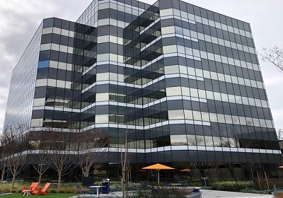
San Jose Office Overview
- Location: The Concourse, 1731 Technology Drive, Suite 595, San Jose, CA 95110 U.S.A.
- Telephone number: 1-408-821-2705
- Installation date: June 1, 2019
About Taiyo America
For over 29 years, Taiyo America, Inc., a subsidiary of Taiyo Holdings Co., Ltd. has propelled itself into the latest technologies and trends, and continues to use its extensive worldwide R&D resources to further offerings and capabilities that include the latest in specialty dielectric inks and via filling inks for use with microvia and build-up technologies, as well as thermal-cure and UV-cure solder masks, Inkjet and Packaging inks. New offerings include inkjet solder mask, dielectric and conductive ink products for the printed electronics and lighting and displays markets. For more information, go to www.taiyoamerica.com.
About Taiyo Holdings Co. Ltd – Est. 1953
The World's Leading Manufacturer of Solder Resist
A specialty chemical manufacturer that proudly holds a top-class share in the global market for solder resist, a material that forms an essential component of the printed wiring boards used in cellular phones, computers, and other IT equipment, as well as in digital home electronics, in electronic equipment installed in automobiles, and a variety of other electronic devices. For more information, go to www.taiyo-hd.co.jp/en/
Share on:


Testimonial
"We’re proud to call I-Connect007 a trusted partner. Their innovative approach and industry insight made our podcast collaboration a success by connecting us with the right audience and delivering real results."
Julia McCaffrey - NCAB GroupSuggested Items
BTU International Earns 2025 Step-by-Step Excellence Award for Its Aqua Scrub™ Flux Management System
10/29/2025 | BTU International, Inc.BTU International, Inc., a leading supplier of advanced thermal processing equipment for the electronics manufacturing market, has been recognized with a 2025 Step-by-Step Excellence Award (SbSEA) for its Aqua Scrub™ Flux Management Technology, featured on the company’s Pyramax™ and Aurora™ reflow ovens.
Rehm Wins Mexico Technology Award for CondensoXLine with Formic Acid
10/17/2025 | Rehm Thermal SystemsModern electronics manufacturing requires technologies with high reliability. By using formic acid in convection, condensation, and contact soldering, Rehm Thermal Systems’ equipment ensures reliable, void-free solder joints — even when using flux-free solder pastes.
Indium Experts to Deliver Technical Presentations at SMTA International
10/14/2025 | Indium CorporationAs one of the leading materials providers to the power electronics assembly industry, Indium Corporation experts will share their technical insight on a wide range of innovative solder solutions at SMTA International (SMTAI), to be held October 19-23 in Rosemont, Illinois.
Knocking Down the Bone Pile: Revamp Your Components with BGA Reballing
10/14/2025 | Nash Bell -- Column: Knocking Down the Bone PileBall grid array (BGA) components evolved from pin grid array (PGA) devices, carrying over many of the same electrical benefits while introducing a more compact and efficient interconnect format. Instead of discrete leads, BGAs rely on solder balls on the underside of the package to connect to the PCB. In some advanced designs, solder balls are on both the PCB and the BGA package. In stacked configurations, such as package-on-package (PoP), these solder balls also interconnect multiple packages, enabling higher functionality in a smaller footprint.
Indium to Showcase High-Reliability Solder and Flux-Cored Wire Solutions at SMTA International
10/09/2025 | Indium CorporationAs one of the leading materials providers in the electronics industry, Indium Corporation® will feature its innovative, high-reliability solder and flux-cored wire products at SMTA International (SMTAI), to be held October 19-23 in Rosemont, Illinois.