


 The Marketing Minute: Marketing With Layers
 The Right Approach: Electro-Tek—A Williams Family Legacy, Part 1
 It’s Only Common Sense: If You’re Not Differentiated, You’re Dead


3D Printing Technique Accelerates Nanoscale Fabrication a Thousandfold
October 4, 2019 | Georgia Institute of TechnologyEstimated reading time: 4 minutes
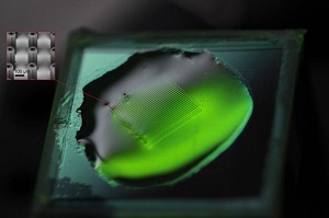
Using a new time-based method to control light from an ultrafast laser, researchers have developed a nanoscale 3D printing technique that can fabricate tiny structures a thousand times faster than conventional two-photon lithography (TPL) techniques, without sacrificing resolution.
Despite the high throughput, the new parallelized technique—known as femtosecond projection TPL (FP-TPL)—produces depth resolution of 175 nanometers, which is better than established methods and can fabricate structures with 90-degree overhangs that can’t currently be made. The technique could lead to manufacturing-scale production of bioscaffolds, flexible electronics, electrochemical interfaces, micro-optics, mechanical and optical metamaterials, and other functional micro- and nanostructures.
The work, reported October 3 in the journal Science, was done by researchers from Lawrence Livermore National Laboratory (LLNL) and The Chinese University of Hong Kong. Sourabh Saha, the paper’s lead and corresponding author, is now an assistant professor in the George W. Woodruff School of Mechanical Engineering at the Georgia Institute of Technology.
Existing nanoscale additive manufacturing techniques use a single spot of high-intensity light—typically around 700 to 800 nanometers in diameter—to convert photopolymer materials from liquids to solids. Because the point must scan through the entire structure being fabricated, the existing TPL technique can require many hours to produce complex 3D structures, which limits its ability to be scaled up for practical applications.
“Instead of using a single point of light, we project a million points simultaneously,” said Saha. “This scales up the process dramatically because instead of working with a single point that has to be scanned to create the structure, we can use an entire plane of projected light. Instead of focusing a single point, we have an entire focused plane that can be patterned into arbitrary structures.”
To create a million points, the researchers use a digital mask similar to those used in projectors to create images and videos. In this case, the mask controls a femtosecond laser to create the desired light pattern in the precursor liquid polymer material. The high-intensity light causes a polymerization reaction that turns the liquid to solid, where desired, to create 3D structures.
Each layer of the fabricated structure is formed by a 35-femtosecond burst of high-intensity light. The projector and mask are then used to create layer after layer until the entire structure is produced. The liquid polymer is then removed, leaving behind the solid. The FP-TPL technique allows the researchers to produce in eight minutes a structure that would take several hours to produce using earlier processes.
“The parallel two-photon system that has been developed is a breakthrough in nanoscale printing that will enable the remarkable performance in materials and structures at this size scale to be realized in usable components,” said LLNL’s Center for Engineered Materials and Manufacturing Director Chris Spadaccini.
Unlike consumer 3D printing that uses particles sprayed onto a surface, the new technique goes deep into the liquid precursor, allowing the fabrication of structures that could not be produced with surface fabrication alone. For instance, the technique can produce what Saha calls an “impossible bridge” with 90-degree overhangs and with more than a 1,000:1 aspect ratio of length to feature size. “We can project the light to any depth that we want in the material, so we can make suspended 3D structures,” he said.
The researchers have printed suspended structures a millimeter long between bases that are smaller than 100 microns by 100 microns. The structure doesn’t collapse while being fabricated because the liquid and solid are about the same density—and the production happens so quickly that the liquid doesn’t have time to be disturbed.
Beyond bridges, the researchers made a variety of structures chosen to demonstrate the technique, including micro-pillars, cuboids, log-piles, wires and spirals. The researchers used conventional polymer precursors, but Saha believes the technique would also work for metals and ceramics that can be generated from precursor polymers.
“The real application for this would be in industrial-scale production of small devices that may be integrated into larger products, such as components in smartphones,” he said. “The next step is to demonstrate that we can print with other materials to expand the material palette.”
Research groups have been working for years to accelerate the two-photon lithography process used to produce nanoscale 3D structures. The success of this group came from adopting a different way of focusing the light, using its time-domain properties, which allowed production of very thin light sheets capable of high resolution—and tiny features.
Use of the femtosecond laser allowed the research team to maintain enough light intensity to trigger the two-photon process polymerization while keeping the point sizes thin. In the FP-TPL technique, the femtosecond pulses are stretched and compressed as they pass through the optical system to implement temporal focusing. The process, which can generate 3D features smaller than the diffraction-limited, focused light spot, requires that two photons hit the liquid precursor molecules simultaneously.
“Traditionally, there are tradeoffs between speed and resolution,” Saha said. “If you want a faster process, you would lose resolution. We have broken this engineering tradeoff, allowing us to print a thousand times faster with the smallest of features.”
At Georgia Tech, Saha intends to continue advancing the work with new materials and further scale-up of the process.
“So far, we have shown that we can do pretty well on speed and resolution,” he said. “The next questions will be how well we can predict the features and how well we can control the quality over large scales. That will require more work to understand the process itself.”
Share on:


Testimonial
"Advertising in PCB007 Magazine has been a great way to showcase our bare board testers to the right audience. The I-Connect007 team makes the process smooth and professional. We’re proud to be featured in such a trusted publication."
Klaus Koziol - atgSuggested Items
The Marketing Minute: Marketing With Layers
10/15/2025 | Brittany Martin -- Column: The Marketing MinuteMarketing to a technical audience is like crafting a multilayer board: Each layer serves a purpose, from the surface story to the buried detail that keeps everything connected. At I-Connect007, we’ve learned that the best marketing campaigns aren’t built linearly; they’re layered. A campaign might start with a highly technical resource, such as an in-depth article, a white paper, or a podcast featuring an engineer delving into the details of a process. That’s the foundation, the substance that earns credibility.
Taking Control of PCB Verification One Step at a Time
10/09/2025 | Kirk Fabbri, Siemens EDAToday’s designs are as complex as ever, and engineers face tough decisions every day. Simulation and verification teams are confronted with a three-fold challenge: understanding the underlying theory, mastering the tools, and applying best practices.Engineers need to navigate a vast and ever-changing cast of design and simulation tools, often with overlapping functionality.
Happy’s Tech Talk #43: Engineering Statistics Training With Free Software
10/06/2025 | Happy Holden -- Column: Happy’s Tech TalkIn over 50 years as a PCB process engineer, the one skill I acquired in college that has been most beneficial is engineering statistics. Basic statistics was part of my engineering fundamentals classes, but I petitioned the dean to let me take the engineering statistics graduate course because I was creating a senior thesis for my honors focus and needed more training on Design of Experiments (DOE).
Connect the Dots: Evolution of PCB Manufacturing—Lamination
10/02/2025 | Matt Stevenson -- Column: Connect the DotsWhen I wrote The Printed Circuit Designer's Guide to...™ Designing for Reality, it was not a one-and-done effort. Technology is advancing rapidly. Designing for the reality of PCB manufacturing will continue to evolve. That’s why I encourage designers to stay on top of the tools and processes used during production, to ensure their designs capitalize on the capabilities of their manufacturing partner.
Empower Sets New Benchmark with 20x Faster Response and Breakthrough Sustainability Demonstrated at OCP Global Summit 2025
09/25/2025 | Empower SemiconductorEmpower Semiconductor, the world leader in powering AI-class processors, announced that its Crescendo chipset, an artificial intelligence (AI) and high-performance computing (HPC) processor true vertical power delivery platform, is available now for final sampling, with mass production slated for late 2025.