


 Dan’s Biz Bookshelf: ‘Abundance: How We Build a Better Future’
 Trouble in Your Tank: In Complex Systems, Design Rules Aren’t Optional
 It’s Only Common Sense: The Phone Is Still Your Competitive Advantage


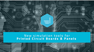
Elsyca Introduces New Simulation Tools for PCB Copper Balancing
April 6, 2020 | ElsycaEstimated reading time: 1 minute
Copper plating is a very complex process that is impacted by the PCB design itself, by the panel layout and by the production configuration.
The ever-increasing complexity of the design and request to deliver in shorter amounts of time are even pushing experts to—and over—their limits.
In order to support the different players in this process, Elsyca has developed a new product suite for the PCB industry. One of the products, Elsyca PCBBalance will not only provide detailed information on the layer thickness distribution, but also optimizes PCB designs/panels for manufacturing through intelligent copper balancing.
In regard to copper balancing and its importance, Rick Hartley, Principal Engineer of RHartley Enterprises commented, “Copper balancing should be done, not only at the panel level in PCB FAB, but every PCB designer should be taught the many benefits of copper balancing and incorporate the concepts into their board designs.”
Elsyca’s PCBBalance simulation software allows users to master quality by providing detailed feedback on the layer thickness distribution and on top of that, also by generating the most performant copper balancing with a single mouse click.
The most critical areas on the panel will be identified, focusing testing resources on where they are most needed.
Key features include:
- DFM
- Identify layer thickness distribution over boards and panels
- Automated and optimized copper balancing
- Identify the most critical holes for post-production quality testing
- Compare different PCB design and panel layouts side by side
- Download copper balancing results
Click on the appropriate link below to find out how this software will help you in your specific role as a PCB Designer, CAM Engineer or Process Engineer.
To learn even more about Elsyca PCBBalance, download a copy of their white paper or find out in one of their webinars how simple it works.
Share on:


Testimonial
"Our marketing partnership with I-Connect007 is already delivering. Just a day after our press release went live, we received a direct inquiry about our updated products!"
Rachael Temple - AlltematedSuggested Items
Driving Innovation: Selecting the Right Laser Source
04/28/2026 | Simon Khesin -- Column: Driving InnovationWhen I first joined Schmoll Maschinen, I brought experience from almost every PCB process, except for laser. As I immersed myself in laser processing, I realized why it can seem so daunting to a newcomer. The complexity arises from three intersecting factors: A vast variety of laser sources: CO2, UV-nano, green-pico, UV-pico, IR-pico, and others; a diverse range of applications: Drilling, cutting, ablation, and more; and an extensive list of materials: These have vastly different absorption rates. Choosing the right machine or laser source is rarely trivial. Even for experienced engineers, answering "Which source is best?" requires examining the business's specific goals.
Institute of Circuit Technology Spring Seminar 2026: A Bright Future in Europe
04/23/2026 | Pete Starkey, I-Connect007Through the leafy lanes and spring flowers of Warwickshire and back to Meridan, the traditional centre of England, and now officially part of the Metropolitan Borough of Solihull in the county of the West Midlands, I attended the Annual General Meeting and Spring Seminar of the Institute of Circuit Technology (ICT) on April 14. Out of the AGM came notable changes in leadership at the top of the Institute: the retirement of Mat Beadel as chair and Emma Hudson as technical director. Effective May 1, Steve Driver is the new chair, and Alun Morgan is the new technical director.
ACCM Unveils Negative and Near-zero CTE Materials for Large-Format AI Chips
04/21/2026 | Advanced Chip and Circuit MaterialsAdvanced Chip and Circuit Materials, Inc. (ACCM) has launched two new materials: Celeritas HM50, with a negative coefficient of thermal expansion (CTE) of -8 ppm/°C to offset the positive CTE and expansion of copper with temperature on circuit boards, and Celeritas HM001, with near-zero CTE and the low-loss performance needed for high-speed signal layers to 224 Gb/s and faster in artificial intelligence (AI) circuits.
Fresh PCB Concepts: Designing PCBs for Harsh Environments—Reliability Is Engineered Upstream
04/23/2026 | Team NCAB -- Column: Fresh PCB ConceptsWhen engineers hear the phrase “harsh environment,” they usually think of the extreme temperature swings, vibration and shock, pressure changes, or radiation in aerospace. However, aerospace is not the only harsh environment where electronic assemblies must survive. Automotive power electronics, downhole oil and gas tools, marine controls, rail systems, defense platforms, and industrial automation equipment all expose PCBs to environments that are equally unforgiving. The stress mechanisms may differ, but the physics does not.
Advanced Packaging for AI: Reliability Starts at the Cu/Cu/Cu Microvia Junction
04/20/2026 | Kuldip Johal, MKS' AtotechThe rapid growth of AI computing, from training clusters to inference at scale, is reshaping demand across the entire electronics supply chain. Advances in technology requirements, such as higher bandwidth, lower latency, and greater compute density, are driving the development of advanced packaging technologies and transforming the PCB industry across design, manufacturing, testing, and even architecture.