


 Trouble in Your Tank: Implementing Direct Metallization in Advanced Substrate Packaging
 It’s Only Common Sense: Storytelling That Sells—Stop Pitching, Start Painting Pictures
 The Right Approach: Get Ready for ISO 9001 Version 6


Real Time with… AltiumLive Europe: If You Don’t Know How It’s Made, How Can You Possibly Design It?
October 26, 2020 | Pete Starkey, I-Connect007Estimated reading time: 4 minutes

Designers attending the AltiumLive Europe 2020 Virtual Summit had the opportunity to see at first-hand how circuit boards were made to help them make informed design-for-manufacturing decisions.
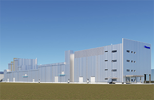
Listed by Michael Gasch as the largest PCB manufacturer in Europe—and certainly one of the most modern, specialising in flex-rigid circuits, embedding technology, and other high-tech solutions—Würth Electronik welcomed AltiumLive to its Niedernhall factory to take a virtual tour. And a team of experts was on hand to provide real-time answers to questions raised by participants—of which there were more than 400.
The session was moderated by Altium multimedia marketing manager Benjamin Kitzinger. Würth PCB specialist Andreas Schilpp led the tour, and his colleagues—Alexander Staudt, Bernt Schroder, and Klaus Schill-Mulack—made up the panel.
The virtual tour was conducted in 10-minute periods, separated by Q&A sessions, and participants were also encouraged to respond to an occasional on-line multiple-choice quiz. The question asked before the start was how many steps there were in producing a 10-layer multilayer in basic technology—click on a number and submit. The answer was 65, to the surprise of a few who clearly had no hands-on experience of PCB fabrication.
Andreas Schilpp set off on his tour, accompanied by a cameraperson. After showing examples of a variety of product types, he began the manufacturing sequence with the issue of inner layer materials, following them into the yellow safelight area for photoresist lamination and laser direct imaging, then developing, acid etching and resist stripping, bonding treatment, and automated optical inspection before lay-up and hot-press bonding.
There was a Q&A break, with questions about the number of employees (approximately 180, covering 24 hours over six days), whether single-image or panelised data was preferred (single-image so that material usage could be optimised by panelisation in-house), and registration systems (post-etch punch and pin lamination for small batch, or optical alignment, spot weld, and mass-lamination for series production).
And a second quiz: What was the smallest drill diameter used in production? The answer was 0.1 mm.
Back on the virtual tour, Schilpp visited the drill shop: X-ray tooling hole optimisation, robotic flash trimming, and edge dressing, and then drilling. For mechanical drilling, there was a choice of single-spindle modules or multi-spindle machines, with 300,000 rpm spindle speed capability—all with auto-loading facilities. Laser drilling was used for microvia HDI and flex-rigid work. The next process was through-hole metallisation before photoresist lamination for outer layer laser direct imaging, followed by copper and tin pattern plating, resist stripping, alkaline etching and tin stripping, spray coating solder mask, and laser direct imaging. He commented that solder mask application and imaging for certain jobs was by 3D printing.
Another Q&A break brought a question about the cost impact of smaller drilled vias, 0.2 mm versus 0.3 mm. The answer was about 10%. There was also a question about improvement in capability since the factory was rebuilt, re-equipped, and re-commissioned in 2016. They said, “The name’s the same, but everything else is new!”
Next, there was a query about the difference between acid and alkaline etching—acid for photoresist, and alkaline for tin resist. Was copper reclaimed? Yes, copper was recovered from etchant and sent for recycling. What data format was preferred? Würth received about 250 data sets per day and was equipped to accept any format—typically extended Gerber or ODB++; IPC 2581 was seen occasionally but was not expected to replace Gerber. What were the benefits of 3D printing of solder mask? All of the benefits associated with additive processing, and the technology was becoming more widely used.
The third quiz question was about the volume of rinse water used per day, with a choice of answers from 200–20,000 cubic metres. Opinions were widespread, but the actual volume was 2,000 cubic metres.
In the final part of the virtual tour, Schilpp visited the finishing department, where electroless nickel immersion gold was the normal choice for flex-rigid work. Controlled-depth routing was used to remove excess rigid material from the flexible areas of flex-rigid circuits, and through-routing was used to profile individual circuits, so they could be removed from the panel. A pico-laser was available for profiling flexible material. Finished circuits were washed and optically inspected, then electrically tested with flying-probe equipment. Samples were release-tested in the laboratory before final inspection and shipping.
A concluding Q&A session responded to queries about providing customers with manufacturing design rules, including whether electrical testing was carried out 100% as standard (yes), what alternative profiling methods were available (V-scoring, sawing), what extra steps were involved when controlled impedance was required (several, beginning with calculating the stackup), and whether laser drilling would replace mechanical drilling. In all, 120 questions were answered live before time ran out, and several more would subsequently be responded to by email.
The closing quiz question was to guess the approximate cost of a PCB manufacturing plant with a capacity of 400 square metres per day. Most participants underestimated the actual cost of US$175 million!
It was a most informative hour and a quarter! Thank you, Würth Electronik and AltiumLive Europe.
Share on:


Testimonial
"Advertising in PCB007 Magazine has been a great way to showcase our bare board testers to the right audience. The I-Connect007 team makes the process smooth and professional. We’re proud to be featured in such a trusted publication."
Klaus Koziol - atgSuggested Items
Koh Young, Fuji, and Kurtz ERSA Drive Smart Manufacturing Solutions for EV and Automotive Electronics at Kunshan, China Technical Seminar
09/11/2025 | Koh YoungKoh Young Technology, the global leader in True 3D measurement-based inspection solutions, partnered with Fuji Corporation and Kurtz ERSA to host an exclusive technical seminar for leading automotive manufacturers in East China. Held on September 4 at Fuji’s factory in Kunshan, the event gathered participants representing over 35 companies.
MacDermid Alpha Presents at SMTA New Delhi, Bangalore Chapter, on Flux–OSP Interaction
09/09/2025 | MacDermid Alpha Electronics SolutionsMacDermid Alpha contributes technical insights on OSP solderability at the Bangalore Chapter, SMTA reinforcing commitment to knowledge-sharing and industry collaboration.
Electra’s ElectraJet EMJ110 Inkjet Soldermask Now in Black & Blue at Sunrise Electronics
09/08/2025 | Electra Polymers LtdFollowing the successful deployment of Electra’s Green EMJ110 Inkjet Soldermask on KLA’s Orbotech Neos™ platform at Sunrise Electronics in Elk Grove Village, Illinois, production has now moved beyond green.
Absolute EMS: The Science of the Perfect Solder Joint
09/05/2025 | Absolute EMS, Inc.Absolute EMS, Inc., a six-time award-winning provider of fast turnaround, turnkey contract electronic manufacturing services (EMS), is drawing attention to the critical role of 3D Solder Paste Inspection (SPI) in ensuring the reliability of both FLEX and rigid printed circuit board assemblies (PCBAs).
Indium Corporation to Highlight High-Reliability Solder Solutions at SMTA Guadalajara Expo
09/04/2025 | Indium CorporationIndium Corporation, a leading materials refiner, smelter, manufacturer, and supplier to the global electronics, semiconductor, thin-film, and thermal management markets, will feature a range of innovative, high-reliability solder products for printed circuit board assembly (PCBA) at the SMTA Guadalajara Expo and Tech Forum, to be held September 17-18 in Guadalajara, Mexico.