


 Global PCB Connections: Rigid-flex and Flexible PCBs—The Backbone of Modern Electronics
 Flexible Thinking: The Key to a Successful Flex Circuit Design Transfer
 Happy’s Tech Talk #29: Bend-to-Install Semi-flex FR-4


Toward Imperceptible Electronics That You Cannot See or Feel
January 11, 2021 | Osaka UniversityEstimated reading time: 1 minute
Transparent electronics—such as head-up displays that allow pilots to read flight data while keeping their eyes ahead of them—improve safety and allow users to access data while in transit. For healthcare applications, the electronics need to not only be cheap and straightforward to fabricate, but also sufficiently flexible to conform to skin. Silver nanowire networks meet these criteria. However, current methods of development create random nanowire alignment that's insufficient for advanced applications.
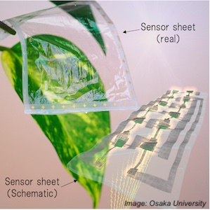
In an upcoming study in Advanced Intelligent Systems, researchers from Osaka University have used high-resolution printing to fabricate centimeter-scale cross-aligned silver nanowire arrays, with reproducible feature sizes from 20 to 250 micrometers. As a proof-of-concept for functionality, they used their arrays to detect electrophysiological signals from plants.
The researchers first created a patterned polymer surface to define the subsequent nanowire feature size. Using a glass rod to sweep silver nanowires across the pattern led to either parallel or cross-aligned nanowire networks, depending on the direction of the sweep. Nanowire cross-alignment, alignment within the pattern, and electro-optical properties were impressive.
"The sheet resistance of patterns less than 100 micrometers ranged from 25 to 170 ohms per square, and the visible light transmittance at 550 nanometers was 96% to 99%," says Teppei Araki, co-senior author. "These values are well-suited for transparent electronics."
The researchers showed off the utility of their technology by monitoring the electric potential of Brazilian waterweed leaves. Because the nanowire arrays are transparent, the researchers were able to keep the leaf under visual observation while acquiring data over long periods of time. A 2- to 3-micrometer-thick device conformed to the surface of a leaf without causing damage.
"Our microelectrodes-based organic field-effect transistors exhibited excellent multi-fuctionality," says Tsuyoshi Sekitani, co-senior author. "For example, transparency of 90%, the on–off ratio was ~106, and the leakage current remained stable upon bending at a radius of 8 millimeters."
Transparent electronics is an emerging technology. It must be simple and inexpensive to mass-produce for biomedicine, civil engineering, agriculture, and other applications that require underlying visual observation. The advance described here is an important step in that direction. The Osaka University researchers plan on making further technical improvements, such as incorporating graphene onto the nanowire’s surface. This will improve the uniformity of the microelectrodes' sheet resistance. Ultimately, the researchers' technology will help minimize the raw material input of electronics, and exceed the functionality of conventional non-transparent electronics.
Read the original article, here.
Share on:


Testimonial
"Advertising in PCB007 Magazine has been a great way to showcase our bare board testers to the right audience. The I-Connect007 team makes the process smooth and professional. We’re proud to be featured in such a trusted publication."
Klaus Koziol - atgSuggested Items
Advanced Semiconductor Packaging Market Sees Rising Adoption Across Automotive and Industrial Sectors
10/14/2025 | openPRThe semiconductor packaging market size is estimated to reach at a CAGR of 7.2% during the forecast period (2024-2031).
Imec Launches 300mm GaN Program to Develop Advanced Power Devices and Reduce Manufacturing Costs
10/13/2025 | ImecImec, a world-leading research and innovation hub in nanoelectronics and digital technologies, welcomes AIXTRON, GlobalFoundries, KLA Corporation, Synopsys, and Veeco as first partners in its 300mm gallium-nitride (GaN) open innovation program track for low- and high-voltage power electronics applications.
NEDME Returns October 22 — The Northwest’s Premier Design & Manufacturing Expo
10/13/2025 | NEDMEThe Northwest Electronics Design & Manufacturing Expo (NEDME) returns on Wednesday, October 22, 2025, at Wingspan Event & Conference Center, Hillsboro. The event brings together engineers, product designers, manufacturers, educators, and community partners for a full day of industry connection, learning, and networking.
Critical Minerals: The New Power Play in Global Trade
10/13/2025 | Marcy LaRont, I-Connect007Access to critical minerals essential for electronics manufacturing, and China’s monopoly of them, is increasingly under scrutiny, with gallium (Ga) and germanium (Ge)at the forefront of this discourse. However, all critical minerals imported from China share a similar narrative, and understanding the implications of this dependency and the risks to both U.S. commercial and defense sectors has created an urgent need for a comprehensive electronics strategy to secure and diversify access to these vital minerals. In this candid interview, USPAE Executive Director Jim Will discusses the issues and the mitigation steps that must be taken to adequately address them.
Precision PCB Acquires Assets of Microplace
10/13/2025 | Precision Technologies Inc.Precision Technologies Inc., doing business as Precision PCB, a One-Stop PCB Fabrication and Assembly services company with 27 years of experience providing Quality, Reliability and Excellence in customer service, has acquired the assets of Microplace, Inc.