


 Driving Innovation: Mechanical and Optical Processes During Rigid-flex Production
 It’s Only Common Sense: Your Biggest Competitor Is Complacency
 The Chemical Connection: Onshoring PCB Production—Daunting but Certainly Possible


PCB Technologies Develops Substrate Integration for Miniaturization
September 29, 2021 | PCB Technologies Ltd.Estimated reading time: 1 minute
In the endless pursuit of miniaturization of microelectronic devices, aimed at their enhanced functionality and reliability in parallel to higher endurance, PCB Technologies has developed the ultimate substrate integration, relevant for various applications.
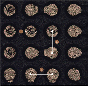
The High-Density substrate in the picture below is based on a unique production technology. A four stack up layered PCB in total height of 260 – 300 µm.
Furthermore, its dialectical spacing is 50 µm (Z axis), while a typical µBGA package has a pitch of about 400 µm and its line spacing is 2.0 - 2.5 mil (X/Y axis), enabling high density assembly.
The PCB’s via construction allows for drilling through more than just one layer of copper. This capability of miniaturization is achieved by several proprietary processes and equipment, one of them is based on utilizing laser direct image camera and a new laser drill machine, maximizing the accuracy of the PCB design and manufacturing.
To top it all, the time it took our engineering team to come up with the final prototype, pending on customer’s feedback and trials at our end, was only 18-20 days!
This product is fully qualified by one of the most advanced aerospace companies in the world and is already in low-rate initial production.
Top Layer
Cross Section
Share on:


