


 Driving Innovation: Mechanical and Optical Processes During Rigid-flex Production
 It’s Only Common Sense: Your Biggest Competitor Is Complacency
 The Chemical Connection: Onshoring PCB Production—Daunting but Certainly Possible


High Density Packaging User Group Announces Uyemura Membership
October 18, 2021 | HDP User GroupEstimated reading time: 1 minute
High Density Packaging (HDP) User Group is pleased to announce that Uyemura International (Uyemura) has become a member.
“As our focus expands from our traditional stronghold in PCB processes into complex assembly processes – especially the high frequency and medical device arenas - we look forward to working with HDP member companies,” said Rich DePoto, Uyemura Business Development Manager.
“I am pleased to welcome Uyemura to HDP, joining the outstanding companies working on HDP User Group projects. Their expertise in surface treatment processes for electronics will contribute significantly to several of our projects, especially those focused on high frequency applications and emerging technologies,” said Larry Marcanti, Executive Director of HDP User Group.
About Uyemura
Uyemura is a science company founded in 1848, with core competencies in the development, testing, and manufacture of process chemistries for the PCB, semiconductor, sensor, photonics and medical device industries.
Uyemura has often been characterized as a disruptor – (long before that became a popular term!) Many Uyemura products have re-invented the solutions of the past, often dramatically, rendering legacy products obsolete, and establishing new benchmarks for performance, longevity, and cost management.
Uyemura was the first company in the industry to establish a research laboratory (today, there are 5 worldwide) as an institution for interdisciplinary surface treatment research. Our global R&D activities have generously rewarded the Uyemura brand with the confidence of leading OEMs in virtually every sector.
More information can be found at: https://www.uyemura.com/index.html
About HDP
HDP User Group, a global research and development organization based in Round Rock, Texas, is dedicated to reducing the costs and risks for the Electronics Manufacturing industry when using advanced electronic packaging and assembly. This international industry-led group organizes and conducts R&D programs to address the technical issues facing the industry, including design, printed circuit board manufacturing, electronics assembly, and environmental compliance. HDP User Group maintains additional offices in Singapore and Tokyo.
For more information, visit HDP User Group on the Internet at www.hdpug.org.
Share on:


Testimonial
"Your magazines are a great platform for people to exchange knowledge. Thank you for the work that you do."
Simon Khesin - Schmoll MaschinenSuggested Items
Fresh PCB Concepts: Resilience and Renewal in Domestic PCB Manufacturing
10/30/2025 | Team NCAB -- Column: Fresh PCB ConceptsAs veterans of PCB manufacturing, we have spent much of our careers walking factory floors, examining copper circuits under microscopes, and troubleshooting plating lines when they go awry at 2 a.m. We can say with confidence that PCBs are the unsung heroes of modern life. They’re in everything, from toothbrushes and thermostats to satellites and defense systems.
Rogers Reports Q3 2025 Results
10/30/2025 | Rogers CorporationRogers Corporation announced financial results for the third quarter of 2025.
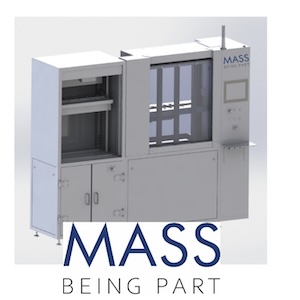
Hofstetter PCB Group Purchases Mass-PCB Vacuum-Filling & Planarising System from Adeon Technologies for New Via Filing Subcontract Services
10/30/2025 | ADEON TechnologiesDuring the Productronica Exhibition in Munich from November 18 through to 21, Adeon is announcing the sale of the newest 2025 model Via Filling equipment with Large Container System and the Planarising system from Mass-PCB to SMF-Hofstetter from Herrenberg, Germany.
Aspocomp’s Interim Report January-September 2025
10/30/2025 | Globe NewswireAspocomp posts interim report for January-September 2025, net sales increased significantly, and the operating result was profitable.
TTM Technologies Reports Q3 2025 Results
10/30/2025 | Globe NewswireTTM Technologies, Inc., a leading global manufacturer of technology products, including mission systems, radio frequency (RF) components, RF microwave/microelectronic assemblies, and technologically advanced printed circuit boards (PCBs) reported results for the third quarter 2025, which ended on September 29, 2025.