


 The Marketing Minute: Cracking the Code of Technical Marketing
 Trouble in Your Tank: Implementing Direct Metallization in Advanced Substrate Packaging


Enpower Greentech Develops World’s Lightest 100 Ah Lithium Metal Battery
July 8, 2022 | PR NewswireEstimated reading time: 1 minute
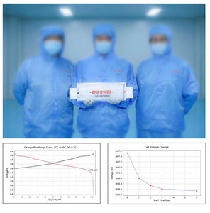
Enpower Greentech Inc. has successfully developed a 100Ah lithium metal battery (LMB), another major step in the commercialization of next-generation batteries for electric vehicles. The breakthrough comes on the heels of Enpower Greentech's newly developed ultra-high energy density (450Wh/kg and 520Wh/kg) LMB in 2021, as well as its safety credentials secured in June 2022.
Enpower Greentech's high-capacity battery cell adopts its proprietary flame-retardant electrolyte solution, which enhances safety without compromising performance. The weight of a single cell is 0.821kg. The cell has a capacity of 102.4Ah (0.1C discharge), a gravimetric energy density of 479Wh/kg, volumetric energy density of 910Wh/L; internal resistance of ?1.0m?. The cell also has a low self-discharge rate (K value ? 2.0?V/h, at 30% SOC), which is less than 10% that of graphite and silicon anode-based traditional lithium-ion batteries.
Enpower Greentech, with subsidiaries in China, Japan, and the U.S., fosters cross-border collaborations to achieve a competitive edge in the development of next generation batteries. It has expanded its product line, developing a 10Ah to 50Ah LMB for the drone and electric aircraft (eVTOL) markets. Enpower Greentech is also developing an all-solid-state LMB and plans to deliver Ah-class pouch cells for external testing by the end of this year. The company plans to start production of 100MWh-scale and GWh-scale LMB manufacturing lines in 2023 and 2024, respectively.
Batteries are now a core technology driving global industry, with multinational automakers and battery manufacturers all competing in the space. On the 10th year of its founding, Enpower Greentech has managed to become a world technology leader, especially with respect to battery performance such as energy density and cycle life. In the future, Enpower will continue to improve its battery performance, optimizing its cycle life, fast-charging, and other performance metrics while reducing costs.
Enpower Greentech's team would like to dedicate their work on safer and better performing batteries to their mentor and collaborator Professor John Goodenough, who celebrates his 100th birthday this month.
Share on:


Testimonial
"The I-Connect007 team is outstanding—kind, responsive, and a true marketing partner. Their design team created fresh, eye-catching ads, and their editorial support polished our content to let our brand shine. Thank you all! "
Sweeney Ng - CEE PCBSuggested Items
Summit Interconnect Announces Appointment of Leo LaCroix as Chief Operating Officer
09/09/2025 | Summit Interconnect, Inc.Summit Interconnect, a leading North American manufacturer of Printed Circuit Boards (PCBs), today announced that Leo LaCroix has assumed the role of Chief Operating Officer (COO).
UHDI Fundamentals: UHDI Technology and Industry 4.0
09/03/2025 | Anaya Vardya, American Standard CircuitsUltra high density interconnect (UHDI) technology is rapidly transforming how smart systems are designed and deployed in the context of Industry 4.0. With its capacity to support highly miniaturized, high-performance, and densely packed electronics, UHDI is a critical enabler of the smart, connected, and automated industrial future. Here, I’ll explore the synergy between UHDI and Industry 4.0 technologies, highlighting applications, benefits, and future directions.
Mastering PCB Floor Planning
08/28/2025 | Stephen V. Chavez, Siemens EDAPlacement of PCB components is far more than just fitting components onto a board. It’s a strategic and critical foundational step, often called “floor planning,” that profoundly impacts the board’s performance, reliability, manufacturability, and cost. Floor planning ties into the solvability perspective, with performance and manufacturability being the other two competing perspectives for addressing and achieving success in PCB design.
Macronix Introduces Cutting-Edge Secure-Boot NOR Flash Memory
08/08/2025 | PRNewswireMacronix International Co., Ltd., a leading integrated device manufacturer in the non-volatile memory (NVM) market, announced ArmorBoot MX76, a robust NOR flash memory combining in a single device, the essential performance and an array of security features that deliver rapid boot times and iron-clad data protection.
UHDI Fundamentals: UHDI Technology and Industry 4.0
08/05/2025 | Anaya Vardya, American Standard CircuitsUltra high density interconnect (UHDI) technology is rapidly transforming how smart systems are designed and deployed in Industry 4.0. With its capacity to support highly miniaturized, high-performance, and densely packed electronics, UHDI is a critical enabler of the smart, connected, and automated industrial future. This article explores the synergy between UHDI and Industry 4.0 technologies, highlighting applications, benefits, and future directions.