


 Global Citizenship: Together for a Perfect PCB Solution
 Smart Automation: Odd-form Assembly—Dedicated Insertion Equipment Matters
 Nolan’s Notes: Everyone Has Their Eye on India


Saki to Showcase 3D AOI, SPI and AXI Solutions at NEPCON Vietnam 2022
September 8, 2022 | Saki CorporationEstimated reading time: 2 minutes
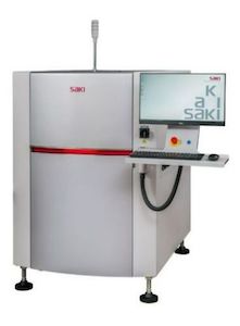
Saki Corporation, an innovator in the field of automated optical and X-ray inspection equipment, is preparing to exhibit at NEPCON Vietnam 2022. From 14 to 16 September, visitors to the Saki booth #H01 will be invited to discover the latest 3D AOI, SPI and AXI inspection solutions alongside its 2D AOI benchtop model BF-Sirius. Together with our partner JS TECH, the Saki technology team will also present latest hard- and software innovations and demonstrate its Full SMT Line, Smart Factory and M2M capabilities.
Visitors to the Saki booth #H01 will be invited to take a first-hand look at the unique features of the latest hardware and software releases with an emphasis on accuracy, speed, reliability and full-line connectivity capability for applications across all sectors.
The show line-up on booth #H01 will feature:
3D-AOI
3D-AOI solution: 3Di-LS2 with 12?m high resolution Z-axis optical head control feature
The 3D AOI model 3Di-LS2 with 12?m camera head is designed to improve production, boost process efficiency, and maximize product quality. Equipped with Saki’s new Z-axis optical-head control feature, the machine’s advanced capabilities for accurate inspection of tall components, press-fit components and PCBAs in jigs will be a key highlight of the show. The innovative optical-head and side camera offers the industry’s highest level of inspection capability with a height-measurement range in 3D mode up to 40mm. The focus height in 2D is also increased to 40mm. With these capabilities, Saki’s 3Di-AOI Series fulfills inspection capabilities and flexibility far beyond standard SMT inspection processes with accuracy, speed, and ease.
3D-SPI
3Si-LD2 with 12?m camera head
Saki’s high-precision and high-speed 3D solder paste inspection machine is a dual-lane system equipped with a 12µm camera head for board sizes from 50mm x 60mm to 500mm x 510mm.
2D-AOI
BF-Sirius – Benchtop Solution for Large size PCB’s
BF-Sirius is a high-speed 2D AOI benchtop model that supports large size PCBs up to 500 x 460 mm (19.7? x 18.1?). The small footprint minimizes cost and floorspace requirements. The system can inspect multiple SMT processes including selective solder and conformal coating.
AXI
Visitors to the booth will also be offered an insight into Saki’s automated X-ray inspection systems that deploy unique Planar CT technology to provide high-speed and high-accuracy solutions for ‘Real 3D’ volumetric inspection. The systems clearly identify voids in the solder of BGAs mounted on boards and non-wetting shapes such as Head-In-Pillow caused by non-wetting of solder, as well as detecting defective parts.
“As one of the world’s top exporting countries of electronics, Vietnam is a key strategic region of focus for Saki,” said Eddie Ichiyama, Saki Chief Sales Manager Overseas. “We’re incredibly excited to be exhibiting again at NEPCON Vietnam after Covid 19 restrictions have finally lifted. We can’t wait to share our expertise and knowledge with the many visitors to the show.”
Share on:


Testimonial
"The I-Connect007 team is outstanding—kind, responsive, and a true marketing partner. Their design team created fresh, eye-catching ads, and their editorial support polished our content to let our brand shine. Thank you all! "
Sweeney Ng - CEE PCBSuggested Items
Koh Young, Fuji, and Kurtz ERSA Drive Smart Manufacturing Solutions for EV and Automotive Electronics at Kunshan, China Technical Seminar
09/11/2025 | Koh YoungKoh Young Technology, the global leader in True 3D measurement-based inspection solutions, partnered with Fuji Corporation and Kurtz ERSA to host an exclusive technical seminar for leading automotive manufacturers in East China. Held on September 4 at Fuji’s factory in Kunshan, the event gathered participants representing over 35 companies.
MacDermid Alpha Presents at SMTA New Delhi, Bangalore Chapter, on Flux–OSP Interaction
09/09/2025 | MacDermid Alpha Electronics SolutionsMacDermid Alpha contributes technical insights on OSP solderability at the Bangalore Chapter, SMTA reinforcing commitment to knowledge-sharing and industry collaboration.
Electra’s ElectraJet EMJ110 Inkjet Soldermask Now in Black & Blue at Sunrise Electronics
09/08/2025 | Electra Polymers LtdFollowing the successful deployment of Electra’s Green EMJ110 Inkjet Soldermask on KLA’s Orbotech Neos™ platform at Sunrise Electronics in Elk Grove Village, Illinois, production has now moved beyond green.
Absolute EMS: The Science of the Perfect Solder Joint
09/05/2025 | Absolute EMS, Inc.Absolute EMS, Inc., a six-time award-winning provider of fast turnaround, turnkey contract electronic manufacturing services (EMS), is drawing attention to the critical role of 3D Solder Paste Inspection (SPI) in ensuring the reliability of both FLEX and rigid printed circuit board assemblies (PCBAs).
Indium Corporation to Highlight High-Reliability Solder Solutions at SMTA Guadalajara Expo
09/04/2025 | Indium CorporationIndium Corporation, a leading materials refiner, smelter, manufacturer, and supplier to the global electronics, semiconductor, thin-film, and thermal management markets, will feature a range of innovative, high-reliability solder products for printed circuit board assembly (PCBA) at the SMTA Guadalajara Expo and Tech Forum, to be held September 17-18 in Guadalajara, Mexico.