


 Trouble in Your Tank: Implementing Direct Metallization in Advanced Substrate Packaging
 It’s Only Common Sense: Storytelling That Sells—Stop Pitching, Start Painting Pictures
 The Right Approach: Get Ready for ISO 9001 Version 6


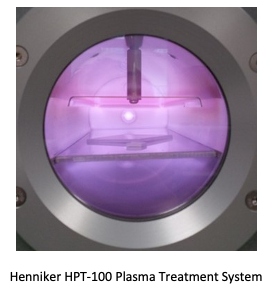
Henniker Plasma: Plasma Treatment of Fluoropolymers
February 14, 2023 | Henniker PlasmaEstimated reading time: 2 minutes
PTFE, and other fluorinated polymers, are chemically inert, thermally stable and highly hydrophobic, due to their intrinsically low surface energy. The chemical inertness of PTFE as an example, means that it is virtually impossible to form lasting adhesive bonds and coatings tend instead to form droplets and 3D particles on the surface rather than a uniform film. Traditional methods to increase the surface energy involve the use of aggressive primers which represent an ecological hazard.
Fluorinated polymers are not readily modified by standard plasma processes. Oxygen plasmas, which are successfully used to treat many hydrocarbon-based polymers, are not successful because the binding energy of the fluorine to carbon atom is far higher than that of oxygen to carbon. Plasma treatment of fluorinated polymers with oxygen plasmas instead causes a gradual etching of the surface, as opposed to surface activation.
The use of hydrogen plasma on the other hand, produces an immediate and lasting change in the nature of the fluoropolymer surface. The action of atomic hydrogen, generated by the plasma, is to react with surface fluorine and remove this into the gas phase where it is pumped away by the vacuum system. Hydrogen then terminates the free surface bonds to produce a CHx polymer surface which is readily wettable. The resulting surface is also mildly-etched on a microscopic scale which produces a microscopically structured surface. Both actions in combination result in a modified surface which may be glued, painted etc.
Typical Results
Results, below and across, show the change in morphology, water contact angle and surface energy obtained for PTFE following hydrogen plasma treatment. The surface energy of PTFE that has been plasma treated is actually lower than that of many common polyolefins, such as polyethylene and polypropylene, and well within the range of wettability required for many adhesives to form strong bonds.
Plasma Process
When gas atoms are ionised, the collision of high energy particles knocks electrons out of their orbits. This results in the characteristic “glow” or light associated with plasma. Plasmas many different species including atoms, molecules, ions, electrons, free radicals, metastables, and photons in the short wave ultraviolet (vacuum UV or VUV) range. Plasmas are generated in closed vessels at low pressures, typically < 1.0 Torr. The low pressure results in a long mean free path of the plasma species, so that they remain reactive until contact with a surface. The overall chamber temperature at the commonly used power levels and pressures is close to room temperature
Share on:


Testimonial
"The I-Connect007 team is outstanding—kind, responsive, and a true marketing partner. Their design team created fresh, eye-catching ads, and their editorial support polished our content to let our brand shine. Thank you all! "
Sweeney Ng - CEE PCBSuggested Items
Driving Innovation: Depth Routing Processes—Achieving Unparalleled Precision in Complex PCBs
09/08/2025 | Kurt Palmer -- Column: Driving InnovationIn PCB manufacturing, the demand for increasingly complex and miniaturized designs continually pushes the boundaries of traditional fabrication methods, including depth routing. Success in these applications demands not only on robust machinery but also sophisticated control functions. PCB manufacturers rely on advanced machine features and process methodologies to meet their precise depth routing goals. Here, I’ll explore some crucial functions that empower manufacturers to master complex depth routing challenges.
Polar Instruments Announces Additive Transmission Line Support for Si9000e
08/20/2025 | Polar InstrumentsTransmission lines embedded into the PCB surface are a feature of UHDI constructions. The 2025 fall release of Polar's Si9000e PCB impedance & insertion loss transmission line field solver incorporates eight new single ended, differential and coplanar transmission line structures.
Henniker Plasma Launches Stratus Turnkey Plasma Manufacturing Cell
08/13/2025 | Henniker PlasmaHenniker Plasma, a leading manufacturer of plasma treatment systems, proudly announces the launch of its Stratus Plasma Manufacturing Cell range — a fully integrated, turnkey solution that combines advanced atmospheric plasma surface treatment with robotic automation.
Trouble in Your Tank: Metallizing Flexible Circuit Materials—Mitigating Deposit Stress
08/04/2025 | Michael Carano -- Column: Trouble in Your TankMetallizing materials, such as polyimide used for flexible circuitry and high-reliability multilayer printed wiring boards, provide a significant challenge for process engineers. Conventional electroless copper systems often require pre-treatments with hazardous chemicals or have a small process window to achieve uniform coverage without blistering. It all boils down to enhancing the adhesion of the thin film of electroless copper to these smooth surfaces.
Designers Notebook: Basic PCB Planning Criteria—Establishing Design Constraints
07/22/2025 | Vern Solberg -- Column: Designer's NotebookPrinted circuit board development flows more smoothly when all critical issues are predefined and understood from the start. As a basic planning strategy, the designer must first consider the product performance criteria, then determine the specific industry standards or specifications that the product must meet. Planning also includes a review of all significant issues that may affect the product’s manufacture, performance, reliability, overall quality, and safety.