


 Dan’s Biz Bookshelf: Four Important Books You Need to Read (Not Just Say You Have)
 Marcy’s Musings: Advancing the Advanced Materials Discussion
 The Marketing Minute: Cracking the Code of Technical Marketing


Production Begins at SEL’s $100M Printed Circuit Board Facility
February 27, 2023 | Schweitzer Engineering LaboratoriesEstimated reading time: 2 minutes
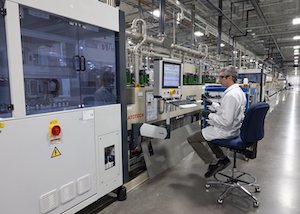
Schweitzer Engineering Laboratories will officially begin fabricating printed circuit boards in its new, state-of-the-art facility in Moscow, Idaho, next week.
The 162,000-square-foot facility, which the company began constructing in spring 2021, will house the operation to fabricate the printed circuit boards used in its products that protect, monitor, control and automate electric power systems around the world. SEL manufactures its electronic devices in Pullman, Washington; Lewiston, Idaho; Lake Zurich, Illinois; and West Lafayette, Indiana.
“SEL folks with many different backgrounds, educations, interests and experience teamed up to conceive, design, build and produce these essential components of our products—all on our own dime without any government handouts or subsidies,” said President and Chief Technology Officer Edmund O. Schweitzer, III. “We committed to each other to do it right, and now we are safely producing the highest-quality boards in the cleanest plant, using the least amount of resources that science and engineering afford us today. This is $100M of employee owners’ money well spent on creating our future right here at home. I’m proud of our entire team and grateful for the economic and political freedom we enjoy in America.”
SEL has designed a highly automated and environmentally friendly process for manufacturing printed circuit boards that is focused on the health and safety of the community. The facility features zero-discharge water recycling and air filtration technology.
“We went into this not only thinking like a manufacturer but also like community members,” said Senior Director of Vertical Integration Jessi Hall. “So much research, learning and testing has gone into designing our fabrication processes and selecting the best equipment and tools for the job. We are excited to see everything come together and to really start realizing the benefits of these investments.”
The company will employ about 60 people in the facility. The positions range from a variety of engineering roles, including chemical, mechanical, software and computer-aided manufacturing to equipment operators and maintenance workers.
The printed circuit board process begins by layering fiberglass and copper to create a rigid and conductive base. The base board is then sent through a series of automated processes that include drilling, layering, copper plating and etching. The finished boards serve as the foundation of our manufacturing process, where integrated circuits and other electrical components are mounted to the board. Ultimately, the boards and added components serve as the information centers for our SEL products.
The SEL property team served as the contractor for the construction project and partnered with multiple companies local to the Pacific Northwest. The team was able to complete the project within the expected timeline despite global supply chain challenges.
“I am so proud of SEL’s partnership with dedicated subcontractors to find solutions when materials became scarce and timelines unwieldy,” said Vice President of Property Jana Schultheis. “Our construction teams are second to none. It is a proud day to see this factory come online as a result of their ingenuity.”
SEL plans to host a grand opening for the facility later in the year.
Share on:


Testimonial
"Our marketing partnership with I-Connect007 is already delivering. Just a day after our press release went live, we received a direct inquiry about our updated products!"
Rachael Temple - AlltematedSuggested Items
Electrodeposited Copper Foils Market to Grow by $11.7 Billion Over 2025-2032
09/18/2025 | Globe NewswireThe global electrodeposited copper foils market is poised for dynamic growth, driven by the rising adoption in advanced electronics and renewable energy storage solutions.
MacDermid Alpha Showcases Advanced Interconnect Solutions at PCIM Asia 2025
09/18/2025 | MacDermid Alpha Electronics SolutionsMacDermid Alpha Electronic Solutions, a global leader in materials for power electronics and semiconductor assembly, will showcase its latest interconnect innovations in electronic interconnect materials at PCIM Asia 2025, held from September 24 to 26 at the Shanghai New International Expo Centre, Booth N5-E30
Trouble in Your Tank: Implementing Direct Metallization in Advanced Substrate Packaging
09/15/2025 | Michael Carano -- Column: Trouble in Your TankDirect metallization systems based on conductive graphite are gaining popularity throughout the world. The environmental and productivity gains achievable with this process are outstanding. Direct metallization reduces the costs of compliance, waste treatment, and legal issues related to chemical exposure. A graphite-based direct plate system has been devised to address these needs.
Closing the Loop on PCB Etching Waste
09/09/2025 | Shawn Stone, IECAs the PCB industry continues its push toward greener, more cost-efficient operations, Sigma Engineering’s Mecer System offers a comprehensive solution to two of the industry’s most persistent pain points: etchant consumption and rinse water waste. Designed as a modular, fully automated platform, the Mecer System regenerates spent copper etchants—both alkaline and acidic—and simultaneously recycles rinse water, transforming a traditionally linear chemical process into a closed-loop system.
Driving Innovation: Depth Routing Processes—Achieving Unparalleled Precision in Complex PCBs
09/08/2025 | Kurt Palmer -- Column: Driving InnovationIn PCB manufacturing, the demand for increasingly complex and miniaturized designs continually pushes the boundaries of traditional fabrication methods, including depth routing. Success in these applications demands not only on robust machinery but also sophisticated control functions. PCB manufacturers rely on advanced machine features and process methodologies to meet their precise depth routing goals. Here, I’ll explore some crucial functions that empower manufacturers to master complex depth routing challenges.