


 Flexible Thinking: Designing Flex Circuits for Dynamic Reliability
 Global PCB Connections: Rigid-flex and Flexible PCBs—The Backbone of Modern Electronics
 Happy’s Tech Talk #29: Bend-to-Install Semi-flex FR-4


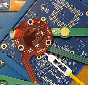
DFM Analysis for Flex and Rigid-flex Design, Part 1
April 17, 2023 | Mark Gallant, DownStream TechnologiesEstimated reading time: 3 minutes

Introduction
Flex and rigid-flex PCB constructions are not new concepts. It has become commonplace as engineers look for alternative circuit packaging for ever-shrinking electronic products. A flat, one-sheet schematic for a straight ribbon cable is analogous to its physical flat substrate. A flat, multi-sheet schematic that details circuitry for a rigid-flex design bears little visual resemblance to its three-dimensional, variable material rigid-flex assembly. However, in both schematic examples, schematic-based analysis tools are applied equally. This same truth also applies to common FR-4-based two-layer or multilayer PCBs.
Today’s PCB analysis tools are applicable across all combinations of rigid PCBs regardless of layer count or size. However, due to the unique properties of flexible substrates and combined flexible and rigid substrates, flexible designs require a specific collection of analysis both functional and manufacture oriented.
Signal integrity analysis such as impedance, coupling, crosstalk and noise is complicated by variable stackups across flexible designs. A single transmission line can be stripline in a rigid-flex area and microstrip in a flex area. Material types and dielectric constants above or below a trace as it traverses a design also vary. While the challenges for signal integrity analysis for flexible designs is worthy of conversation, this article will focus on the current challenges to design-for-manufacture analysis of flex and rigid-flex designs.
Contrasting Rigid PCBs With Flex and Rigid-flex
Some designers design flexible PCBs as simple bendable circuit boards, but there are vast differences between rigid and flexible. Both technologies produce an electrical interconnect function, but are manufactured using different types of materials and processes. They also have varying applications. No need to design a rigid-flexible PCB for the motherboard of a desktop PC, but rigid-flex is required for most medically implanted devices.
A typical rigid PCB is comprised of electrodeposited copper-clad fiberglass substrates bonded together. While there are variations on materials used to bond substrates, it is commonly sheets of cloth pre-impregnated with uncured epoxy. This bonding material composition is not engineered to be flexible. The copper is chemically etched to create a circuit pattern. The hardness of the bonded substrates requires mechanical routing to trim the raw PCBs. All layers of the PCB are commonly identical in size and shape unless cavities, embedded components, or other such exotic construction is present. The rigid PCB layer stackup is identical across the entire PCB area. Solder mask and legend are almost always applied.
Flexible PCBs are comprised of rolled annealed copper over flexible polyimide substrates. Flexible layers or cores are produced with or without adhesives. Adhesiveless flex is prevalent in applications requiring higher performance, while those with adhesives are often found in low layer-count applications. The most common usage is copper foil laminated to a substrate with epoxy or acrylic adhesive. Both substrate material and adhesive are engineered for bending to minimize trace fracture. Like rigid PCBs, a chemical etching process is used to create a circuit pattern. The flexible nature of the materials requires die cutting or “blanking” rather than mechanical routing. Each layer of a flexible double-sided core has an identical shape.
However, multilayer flex is likely to have variations in shape for each layer or core. Flexible PCBs require a thin film insulator over the conductors know as a coverlay. Unlike rigid PCB solder masks, coverlays are die cut much like the flexible layers they insulate. The stackup of a multi-layer flexible PCB can vary across the PCB area. This is especially true with multilayer flex where layer shape varies among the collection of layers or cores. A flexible ground or power plane area is typically crosshatched versus solid for rigid PCBs. The crosshatch reduces potential for fracture of conductors. Alternatively, flexible layers can be shielded with a layer of copper or silver foil. Masking and screening over flexible layers is not rare, but uncommon.
To read this entire article, which appeared in the April 2023 issue of Design007 Magazine, click here.
Share on:


Testimonial
"The I-Connect007 team is outstanding—kind, responsive, and a true marketing partner. Their design team created fresh, eye-catching ads, and their editorial support polished our content to let our brand shine. Thank you all! "
Sweeney Ng - CEE PCBSuggested Items
SMTA Ultra HDI Symposium, Day 2: Fragile Supply Chains, Fierce Innovation
04/14/2026 | Marcy LaRont, I-Connect007The Arizona weather yielded another beautiful day as we gathered for the second day of SMTA’s annual UHDI symposium. After the first full day discussing the role of AI in business and the how-tos of implementation, Avondale Mayor Mike Pineda kicked off day two, proud to showcase his city and to declare its important place in the continued development of the West Valley, an increasingly important area for tech and manufacturing.
KYZEN Focuses on Aqueous and Stencil Cleaning Solutions at SMTA Monterrey Expo and Tech Forum
04/10/2026 | KYZEN'KYZEN, the global leader in innovative environmentally friendly cleaning chemistries, will exhibit at the SMTA Monterrey Expo & Tech Forum.
Solder Paste Innovations for Enhanced Reliability from MacDermid Alpha Electronics Solutions
04/10/2026 | Real Time with... APEX EXPOJason Fullerton of MacDermid Alpha Electronics Solutions discusses innovative alloys like Innolot MXE, low-temperature solder options, and polymer reinforcement strategies. Learn how these solutions address the growing demands of high-performance computing and larger component assemblies, ensuring optimal performance and cost-effectiveness.
Frank Sommer Discusses Selective Soldering Innovations for EVs
04/10/2026 | Real Time with... APEX EXPODan Beaulieu sits down with Frank Sommer, a selective soldering expert from Nordson Electronics Solutions, to discuss the resurgence of selective soldering driven by electric vehicle manufacturing, and the need for robust through-hole component integration. He also introduces Nordson's innovative SELECT Synchro selective soldering machine, designed for enhanced throughput and flexibility.
Double Win: Indium Corporation’s CW-807RS and Indium12.9HF Receive EM Asia Innovation Honors
04/07/2026 | Indium CorporationIndium Corporation®, a leading materials provider for the electronics assembly market, recently received Electronics Manufacturing (EM) Asia Innovation Awards for its halogen-free CW-807RS flux-cored wire and Indium12.9HF solder paste products.