


 Flexible Thinking: Designing Flex Circuits for Dynamic Reliability
 Global PCB Connections: Rigid-flex and Flexible PCBs—The Backbone of Modern Electronics
 Happy’s Tech Talk #29: Bend-to-Install Semi-flex FR-4


iNEMI Call-for-Participation Webinar: PCB Connector Footprint Tolerance Project
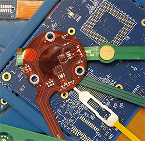
May 4, 2023 | iNEMIEstimated reading time: 1 minute

Size reduction coupled with increased bandwidth is driving new and tighter PCB/FPC (flexible printed circuit) design requirements that may exceed the capability of fabrication processes used for previous generations of I/O connector interfaces. In short, connector land pattern tolerances drive process requirements not previously needed. An understanding of complex process interactions is necessary to identify processes to use, conduct risk assessment, and meet product quality requirements.
The purpose of iNEMI’s PCB Connector Footprint Tolerance project is to define methods that enable designers who are creating products with high I/O bandwidth connector footprints to use the collected industry capability and capacity data to determine appropriate mitigation for the required level of quality for a given product. This fast-turnaround project will:
- Provide better understanding of risks associated with high I/O bandwidth connector footprints
- Enable product designers to conduct risk assessments to determine optimum manufacturing processes to enable PCB suppliers to meet product quality requirements
- Reduce product qualification costs and associated time to market
Registration
Join us for our call-for-participation webinar to learn more about this new project. Two sessions are scheduled and are open to industry; advance registration is required, visit iNEMI's website.
Session 1
Tuesday, May 9, 2023
11:00 am. — 12:00 p.m. EDT (US)
5:00-6:00 p.m. CEST (Europe)
Session 2
Wednesday, May 10, 2023
7:00-8:00 a.m. CST (China)
7:00-8:00 p.m. EDT (US) on May 9
Share on:


Testimonial
"The I-Connect007 team is outstanding—kind, responsive, and a true marketing partner. Their design team created fresh, eye-catching ads, and their editorial support polished our content to let our brand shine. Thank you all! "
Sweeney Ng - CEE PCBSuggested Items
Molex Accelerates Supply Chain Transformation with Celonis AI
04/17/2026 | BUSINESS WIRECelonis, a global leader in Process Intelligence, announced a successful collaboration with Molex, a global electronics leader and connectivity innovator, demonstrating that process context provides the essential foundation for reliable, scalable Enterprise AI.
The Future of Reflow Soldering Is Here
04/16/2026 | Real Time with... APEX EXPOMichael Hanke discusses how Rehm Thermal Systems is revolutionizing thermal solutions in electronics assembly with their innovative flux-free, no-clean soldering process. This is truly a game changing process that eliminates chamber cleaning and streamlines production. Developed with paste suppliers, this advanced technology promises significant time and cost savings while ensuring high-quality results.
At KYZEN, Cleaning is All About Reliability
04/17/2026 | Real Time with... APEX EXPOJason Schwartz discusses KYZEN's advanced cleaning solutions for PCB assembly with Dan Beaulieu at APEX EXPO 2026. KYZEN has a 35-year legacy in defluxing, innovative real-time process control, and commitment to ensuring electronic reliability. How KYZEN partners with manufacturers through process audits and lab testing to maintain optimal cleaning standards is part of this conversation.
Molex Accelerates Supply Chain Transformation with Celonis AI
04/16/2026 | BUSINESS WIRECelonis, a global leader in Process Intelligence, announced a successful collaboration with Molex, a global electronics leader and connectivity innovator, demonstrating that process context provides the essential foundation for reliable, scalable Enterprise AI.
SMTA Announces 2026 STAR Forum Technical Program
04/16/2026 | SMTAThe SMTA announced the finalized program for the High Reliability: Strategic Technology Advancement Research Forum which takes place on May 6-7, 2026 in Olathe, Kansas, USA.