


 The Marketing Minute: Cracking the Code of Technical Marketing
 Trouble in Your Tank: Implementing Direct Metallization in Advanced Substrate Packaging


Ayar Labs Adds $25 Million in Expansion of Its $130 Million Series C
May 25, 2023 | Business WireEstimated reading time: 2 minutes
Ayar Labs, a leader in silicon photonics for chip-to-chip connectivity, announced it has raised an additional $25 million in Series C1 funding, bringing its total Series C raise to $155 million. The oversubscribed up round was led by new investor Capital TEN. VentureTech Alliance also entered the Series C expansion that included participation by previous investors Boardman Bay Capital Management, IAG Capital Partners, NVIDIA, and Tyche Partners. Existing strategic and financial investors include Applied Ventures, GlobalFoundries, Hewlett Packard Pathfinder, Intel Capital and Lockheed Martin Ventures.
“We believe that future computing solutions will include large-scale use of silicon photonics for data communications, and have been following Ayar Labs for some time now,” said Pin-Nan Tseng, General Partner at Capital TEN. “Given our deep expertise in the semiconductor industry and the Taiwan semiconductor ecosystem, we believe Ayar Labs has the technology solution, people, capital, and broad support to lead in the transition from copper to optical interconnects for scale-out computing and memory applications.”
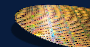
Ayar Labs’ patented optical I/O approach uses industry-standard, cost-effective silicon processing techniques to replace traditional electrical I/O with fast, high-density, low power optical I/O chiplets and multi-wavelength light sources. Moving data between chips using light instead of electricity breaks the performance, power, and distance limitations of copper interconnect, critical for latency-sensitive applications such as high performance computing, AI and machine learning. Optical I/O will also impact other areas that require rapid transfer of data, such as cloud and data center, telecommunications, and aerospace and defense.
“We’re extremely pleased with the ongoing interest and financing we’ve received from leaders in the semiconductor industry,” said Charles Wuischpard, CEO of Ayar Labs. “This C1 adds sophisticated investor partners that will allow us to accelerate our strategic roadmap, and is further validation of our technology and plan to bring silicon photonics-based interconnect solutions to market at scale.”
Ayar Labs will use the funds to accelerate the implementation and commercialization of its optical I/O solutions to address the power consumption, latency, reach and system bandwidth bottlenecks that threaten future advances in generative AI, while also expanding the company's product offerings and development efforts.
NVIDIA, which participated in Ayar Labs’ earlier Series C raise in April 2022, increased its investment in the company.
“NVIDIA is reimagining the data center with integrated hardware, software and networking for accelerated computing,” said Craig Thompson, Vice President of Business Development, Networking Business Unit at NVIDIA. “Generative AI models with trillions of parameters are accelerating demand for this platform, which is why we are increasing our investment in Ayar Labs.”
Recently named one of America’s Best Startup Employers by Forbes, the funds will also help the company increase hiring plans by up to 50 percent this year. Ayar Labs has received a number of other accolades in recent months. The company was recognized as an honoree in Fast Company’s most recent “Next Big Things in Tech” awards. In addition, Mark Wade, Ayar Labs’ Co-Founder, CTO and Senior Vice President of Engineering, was recently appointed to Global Semiconductor Alliance’s CTO Council. Wade was also recently named to Electro Optics’ inaugural “The Photonics 100 2023” list.
Share on:


Testimonial
"We’re proud to call I-Connect007 a trusted partner. Their innovative approach and industry insight made our podcast collaboration a success by connecting us with the right audience and delivering real results."
Julia McCaffrey - NCAB GroupSuggested Items
Trouble in Your Tank: Implementing Direct Metallization in Advanced Substrate Packaging
09/15/2025 | Michael Carano -- Column: Trouble in Your TankDirect metallization systems based on conductive graphite are gaining popularity throughout the world. The environmental and productivity gains achievable with this process are outstanding. Direct metallization reduces the costs of compliance, waste treatment, and legal issues related to chemical exposure. A graphite-based direct plate system has been devised to address these needs.
Closing the Loop on PCB Etching Waste
09/09/2025 | Shawn Stone, IECAs the PCB industry continues its push toward greener, more cost-efficient operations, Sigma Engineering’s Mecer System offers a comprehensive solution to two of the industry’s most persistent pain points: etchant consumption and rinse water waste. Designed as a modular, fully automated platform, the Mecer System regenerates spent copper etchants—both alkaline and acidic—and simultaneously recycles rinse water, transforming a traditionally linear chemical process into a closed-loop system.
Driving Innovation: Depth Routing Processes—Achieving Unparalleled Precision in Complex PCBs
09/08/2025 | Kurt Palmer -- Column: Driving InnovationIn PCB manufacturing, the demand for increasingly complex and miniaturized designs continually pushes the boundaries of traditional fabrication methods, including depth routing. Success in these applications demands not only on robust machinery but also sophisticated control functions. PCB manufacturers rely on advanced machine features and process methodologies to meet their precise depth routing goals. Here, I’ll explore some crucial functions that empower manufacturers to master complex depth routing challenges.
Trouble in Your Tank: Minimizing Small-via Defects for High-reliability PCBs
08/27/2025 | Michael Carano -- Column: Trouble in Your TankTo quote the comedian Stephen Wright, “If at first you don’t succeed, then skydiving is not for you.” That can be the battle cry when you find that only small-diameter vias are exhibiting voids. Why are small holes more prone to voids than larger vias when processed through electroless copper? There are several reasons.
The Government Circuit: Navigating New Trade Headwinds and New Partnerships
08/25/2025 | Chris Mitchell -- Column: The Government CircuitAs global trade winds continue to howl, the electronics manufacturing industry finds itself at a critical juncture. After months of warnings, the U.S. Government has implemented a broad array of tariff increases, with fresh duties hitting copper-based products, semiconductors, and imports from many nations. On the positive side, tentative trade agreements with Europe, China, Japan, and other nations are providing at least some clarity and counterbalance.