


 Trouble in Your Tank: Causes of Plating Voids, Pre-electroless Copper
 Dan’s Biz Bookshelf: ‘Growth Hacker Marketing’
 Happy’s Tech Talk #38: Novel Metallization for UHDI


Keysight Introduces High Density Source Measure Unit to Speed Semiconductor Characterization
July 17, 2023 | Keysight Technologies, Inc.Estimated reading time: 2 minutes
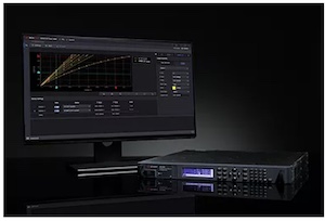
Keysight Technologies, Inc. introduces the PZ2100 Series High-Channel Density Precision Source Measure Unit (SMU) Solution, a new SMU solution giving digital development engineers 20 precision SMU channels within a 1U rack space to speed the characterization of integrated circuit (IC) designs.
While innovation cycles are shortening and digital standards are evolving, designing a semiconductor component or device and delivering it to market remains a time-intensive, technical process. Digital development engineers must connect and test multiple ports on a single device-under-test (DUT) throughout the design cycle to troubleshoot and characterize the performance of the IC. Without high-density, automated characterization solutions, engineers risk slowing their delivery timelines as they validate with complex, multiport designs using complicated and low-density test setups.
Keysight’s PZ2100 Series SMU addresses this risk by giving design engineers a high-density SMU solution that is scalable to 20 SMU channels in a compact 1U rack configuration. The solution also speeds time-to-market with flexible software options, simplified system integration and synchronization, and application-specific measurement capabilities, allowing them to focus more time on characterization and less on synchronization.
The PZ2100 Series SMU delivers the following benefits:
- Single-box solution – Saves time by simplifying channel stacking and synchronization to remove integration and coding complexity. The user-friendly GUI accelerates test prototyping, debugging, and troubleshooting while the PathWave IV Curve Measurement software enables quick measurements and synchronization without programming.
- Scalable, compact, and flexible – Saves rack space by offering up to 20 SMU channels in a valuable 1U full-width form factor that does not require cooling spacers when stacked. Available in five SMU module options that are configurable and upgradeable.
- All-in-one SMU module – Reduces cost by integrating pulser and digitizer functions with conventional SMU functions, such as precise DC voltage and current sourcing and measuring to meet emerging requirements without additional instruments.
Toshio Kimura, General Manager for Furukawa Electric's Next Generation Components Development Department, Next Generation Photonics Business Innovation Project Team, said: "By embedding Keysight's PZ2100 High-Channel Density Precision SMU into our test system, it increases our test throughput for developing and mass-producing optical components for broadband, long-distance transmission. In addition, it helps us reduce our test system footprint with up to 20 channels of SMUs installed in a 1U rack space. This flexible, scalable, and modular solution can also accommodate future test needs, helping to reduce overall test costs. Keysight's extensive product portfolio and metrology expertise drives our business success, allowing us to continue to lead the optical component industry."
Carol Leh, Vice President and General Manager for Keysight's Electronic Industrial Solutions Group's Center of Excellence, said: "With options that scale up to 20 SMU channels, the PZ2100 Series offers five times more channel density than equivalent SMUs, making it the highest channel density SMU in a 1U form factor in the market. Combine this with the PathWave IV Curve software for quick, programming-free IV measurements, and you have a solution that allows you to focus more of your time on actual characterization and less time on synchronization and system bring-up."
Share on:


Suggested Items
AI Chips for the Data Center and Cloud Market Will Exceed US$400 Billion by 2030
05/09/2025 | IDTechExBy 2030, the new report "AI Chips for Data Centers and Cloud 2025-2035: Technologies, Market, Forecasts" from market intelligence firm IDTechEx forecasts that the deployment of AI data centers, commercialization of AI, and the increasing performance requirements from large AI models will perpetuate the already soaring market size of AI chips to over US$400 billion.
NXP Unveils Third-Generation Imaging Radar Processors for Level 2+ to 4 Autonomous Driving
05/09/2025 | NXP SemiconductorNXP Semiconductors N.V. unveiled its new S32R47 imaging radar processors in 16 nm FinFET technology, building on NXP’s proven expertise in the imaging radar space.
OSI Systems Receives $36 Million Contract for Aviation Security Systems
05/08/2025 | BUSINESS WIREOSI Systems, Inc. announced that its Security division received a contract award for approximately $36 million to deploy and service airport screening solutions for a prominent international airport in the Middle East.
Cadence Unveils Millennium M2000 Supercomputer with NVIDIA Blackwell Systems
05/08/2025 | Cadence Design SystemsAt its annual flagship user event, CadenceLIVE Silicon Valley 2025, Cadence announced a major expansion of its Cadence® Millennium™ Enterprise Platform with the introduction of the new Millennium M2000 Supercomputer featuring NVIDIA Blackwell systems, which delivers AI-accelerated simulation at unprecedented speed and scale across engineering and drug design workloads.
Indium’s Karthik Vijay to Present on Dual Alloy Solder Paste Systems at SMTA’s Electronics in Harsh Environments Conference
05/06/2025 | Indium CorporationIndium Corporation Technical Manager, Europe, Africa, and the Middle East Karthik Vijay will deliver a technical presentation on dual alloy solder paste systems at SMTA’s Electronics in Harsh Environments Conference, May 20-22 in Amsterdam, Netherlands.