


 Driving Innovation: Mechanical and Optical Processes During Rigid-flex Production
 It’s Only Common Sense: Your Biggest Competitor Is Complacency
 The Chemical Connection: Onshoring PCB Production—Daunting but Certainly Possible


The Cool Solution to Electronics Heat Dissipation
June 11, 2015 | SLAC National Accelerator LaboratoryEstimated reading time: 3 minutes
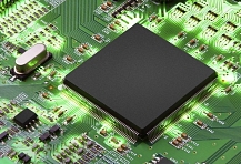
The heat that builds up in the shuttling of current in electronics is an important obstacle to packing more computing power into ever-smaller devices: Excess heat can cause them to fail or sap their efficiency.
Now, X-ray studies at the Department of Energy’s SLAC National Accelerator Laboratory have for the first time observed an exotic property that could warp the electronic structure of a material in a way that reduces heat buildup and improves performance in ever-smaller computer components.
The research was conducted, in part, at SLAC’s Stanford Synchrotron Radiation Lightsource (SSRL), a DOE Office of Science User Facility, and published this month in the print edition of Nature Materials.
Energy-bending Properties
The team studied a form of iridium oxide, Sr3Ir2O7, that belongs to a class of so-called correlated materials in which electrons can be made to behave in sync. It is a candidate for reducing the heat generated by the billions of transistors at the core of modern computers.
The researchers discovered that the material has a long-theorized property, formerly found only in 2-D materials and known as 3-D negative electronic compressibility, that is caused by its unusual electronic structure.
The electronic structure of a material is typically rigid, with distinct energy levels or “bands” that fill up as electrons are added. These levels are determined by the atomic structure and chemical composition of the material. In the study, these energy levels were observed to deform drastically, in a fluid way, as more electrons poured in, while the physical structure of the material did not change in any significant way.
“Imagine pouring water into a cup and watching the water level in the cup appear to dip as the cup deforms,” said Junfeng He, a Boston College researcher who led the study. “That’s how 3-D negative electronic compressibility appears to operate.” But in this case, it is the material’s electronic structure – which defines how it can store or flow electric current – rather than its physical structure that substantially warps as electrons are added.
Guided by theoretical calculations led by Arun Bansil, a professor of physics at Northeastern University, researchers found that a gap between different groupings of energy bands in the sample material actually shrank as electrons were added, reducing the material’s stored energy level – like the water level appearing to decline in the cup example.
In principle, using metal electrodes that have this property in the microscopic gates that regulate the flow of electrons in transistors could substantially enhance their efficiency and reduce heat buildup, said He, who will soon join SLAC as a postdoctoral researcher.
Building a Better Transistor
Rui-Hua He, an assistant professor of physics at Boston College who is a spokesperson for the research, said, “Replacing normal metals in transistors with materials like this that have negative electronic compressibility presents an intriguing alternative to current approaches, with a goal of continuing device miniaturization.” He added, “We are now working on the first demonstration of their potential application to transistors.”
Researchers employed an advanced X-ray technique at SSRL, set up and maintained by SLAC staff scientists Donghui Lu and Makoto Hashimoto, to precisely measure the electronic structure of the material. The negative electronic compressibility they found shows promise for reducing power requirements needed to move electric current around a semiconductor, for example, which would reduce the heat it generates and make electrical switching more efficient.
Previous studies had observed a 2-D version of negative electronic compressibility in other materials, but researchers said the 3-D form has greater potential for application in semiconductors because it is more compatible with their present-day architecture, can potentially be used at room temperature and can be adapted for different applications by adjusting its thickness.
“This work informs us of the importance to continually look for other new materials with novel physical properties for use in transistors and for other applications,” said Stephen Wilson, an assistant professor of materials at the University of California, Santa Barbara, who prepared the sample materials.
Participating researchers were from Boston College, Northeastern University, SLAC’s SSRL and Stanford Institute for Materials and Energy Sciences (SIMES), Lawrence Berkeley National Laboratory, Peking University in China, Hiroshima Synchrotron Radiation Center in Japan and the University of California, Santa Barbara. The work was supported by Boston College, the U.S. National Science Foundation, the W. M. Keck Foundation and the DOE Office of Basic Energy Sciences.
Share on:


Testimonial
"Your magazines are a great platform for people to exchange knowledge. Thank you for the work that you do."
Simon Khesin - Schmoll MaschinenSuggested Items
Sealed for Survival: Potting Electronics for the Toughest Environments
10/29/2025 | Beth Massey, MacDermid Alpha Electronics SolutionsElectronics deployed in harsh conditions face relentless threats from vibration, impact, chemical contaminants, airborne pollutants, and moisture, conditions that can quickly lead to failure without robust protection. Potting, the process of encapsulating electronics in a protective polymer, is a widely used strategy to safeguard devices from both environmental and mechanical hazards.
Driving Innovation: Mechanical and Optical Processes During Rigid-flex Production
10/28/2025 | Kurt Palmer -- Column: Driving InnovationRigid-flex printed circuit boards are a highly effective solution for placing complex circuitry in tight, three-dimensional spaces. They are now indispensable across a range of industries, from medical devices and aerospace to advanced consumer electronics, helping designers make the most efficient use of available space. However, their unique construction—combining rigid and flexible materials—presents a fundamental challenge for PCB manufacturers.
SMTAI 2025 Review: Reflecting on a Pragmatic and Forward-looking Industry
10/27/2025 | Marcy LaRont, I-Connect007Leaving the show floor on the final afternoon of SMTA International last week in Rosemont, Illinois, it was clear that the show remains a grounded, technically driven event that delivers a solid program, good networking, and an easy space to commune with industry colleagues and meet with customers.
ITW EAE Despatch Ovens Now Support ASTM 5423 Testing
10/15/2025 | ITW EAEAs the demand for high-performance electrical insulation materials continues to grow—driven by the rapid expansion of electric vehicles (EVs) and energy storage systems—thermal processing has become a critical step in material development.
Beyond Thermal Conductivity: Exploring Polymer-based TIM Strategies for High-power-density Electronics
10/13/2025 | Padmanabha Shakthivelu and Nico Bruijnis, MacDermid Alpha Electronics SolutionsAs power density and thermal loads continue to increase, effective thermal management becomes increasingly important. Rapid and efficient heat transfer from power semiconductor chip packages is essential for achieving optimal performance and ensuring long-term reliability of temperature-sensitive components. This is particularly crucial in power systems that support advanced applications such as green energy generation, electric vehicles, aerospace, and defense, along with high-speed computing for data centers and artificial intelligence (AI).