


 Dan’s Biz Bookshelf: Four Important Books You Need to Read (Not Just Say You Have)
 The Marketing Minute: Cracking the Code of Technical Marketing


New Technique Enables 3D Mapping of Magnetic Patterns
July 8, 2015 | HZBEstimated reading time: 2 minutes
An international collaboration has succeeded in using synchrotron light to detect and record the complex 3D magnetisation in wound magnetic layers. This technique could be important in the development of devices that are highly sensitive to magnetic fields, such as in medical diagnostics for example. Their results are published now in Nature Communications.
3D structures in materials and biological samples can be investigated today using X-ray tomography. This is done by recording images layer-by-layer and assembling them on a computer into a three-dimensional mapping. But so far there has been no comparable technique for imaging 3D magnetic structures on nm length scales. Now teams from HZB and the Institut für Festkörperphysik / Technische Universität Dresden in collaboration with research partners from institutions in California (1) have developed a technique with which this is possible.
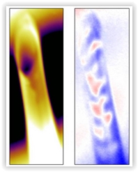
Mapping of rolled-up magnetic samples
They studied the magnetisation in rolled-up tubular magnetic nanomembranes (nickel or cobalt-palladium) about two layers thick. To obtain a 3D mapping of the magnetisation in the tubes, the samples were illuminated with circularly polarized X-rays. Using the X-ray microscope at the Advanced Light Source and the X-ray Photoemission Electron Microscopy (XPEEM) beamline at BESSY II, the samples were slightly rotated for each new image so that a series of 2D images was created. “The polarised light penetrated the magnetic layers from different angles. Using XPEEM, we were not only able to measure the magnetic features at the surface, but also obtained additional information from the “shadow”, explains Florian Kronast, who is responsible for the XPEEM beamline at HZB.
3D reconstruction of magnetic patterns
In the end, the physicists were successful in reconstructing the magnetic features on the computer in three dimensions.
“These samples displayed structures not smaller than 75 nanometres. But with this method we should be able to see even smaller structures and obtain a resolution of 20 nanometres”, explains Florian Kronast. However, so far only electron holography could be considered for mapping magnetic domains of three-dimensional objects at the nanometre scale. This required very complicated sample preparation and the magnetisation could only be indirectly determined through the resulting distribution of the magnetic field. “Our process enables you to map the magnetisation in directly in 3D. Knowledge of the magnetisation is prerequisite for improving the sensitivity of magnetic field detectors.”
Sensors for weak magnetic fields
The new method could be of interest to anyone involved with extremely small magnetic features within small volumes, such as those developing more sensitive devices for medical imaging, for example. Procedures like magnetoencephalography depend on externally detecting very weak magnetic fields created by the electrical activity of individual nerve cells – using appropriately sensitive detectors.
Share on:


Testimonial
"Advertising in PCB007 Magazine has been a great way to showcase our bare board testers to the right audience. The I-Connect007 team makes the process smooth and professional. We’re proud to be featured in such a trusted publication."
Klaus Koziol - atgSuggested Items
MEMS & Imaging Sensors Summit to Spotlight Sensing Revolution for Europe’s Leadership
09/11/2025 | SEMIIndustry experts will gather November 19-20 at the SEMI MEMS & Imaging Sensors Summit 2025 to explore the latest breakthroughs in AI-driven MEMS and imaging optimization, AR/VR technologies, and advanced sensor solutions for critical defence applications.
Direct Imaging System Market Size to Hit $4.30B by 2032, Driven by Increasing Demand for High-Precision PCB Manufacturing
09/11/2025 | Globe NewswireAccording to the SNS Insider, “The Direct Imaging System Market size was valued at $2.21 Billion in 2024 and is projected to reach $4.30 Billion by 2032, growing at a CAGR of 8.68% during 2025-2032.”
I-Connect007’s Editor’s Choice: Five Must-Reads for the Week
07/04/2025 | Marcy LaRont, I-Connect007For our industry, we have seen several bullish market announcements over the past few weeks, including one this week by IDC on the massive growth in the global server market. We’re also closely watching global trade and nearshoring. One good example of successful nearshoring is Rehm Thermal Systems, which celebrates its 10th anniversary in Mexico and the official opening of its new building in Guadalajara.
Driving Innovation: Direct Imaging vs. Conventional Exposure
07/01/2025 | Simon Khesin -- Column: Driving InnovationMy first camera used Kodak film. I even experimented with developing photos in the bathroom, though I usually dropped the film off at a Kodak center and received the prints two weeks later, only to discover that some images were out of focus or poorly framed. Today, every smartphone contains a high-quality camera capable of producing stunning images instantly.
United Electronics Corporation Advances Manufacturing Capabilities with Schmoll MDI-ST Imaging Equipment
06/24/2025 | United Electronics CorporationUnited Electronics Corporation has successfully installed the advanced Schmoll MDI-ST (XL) imaging equipment at their advanced printed circuit board facility. This significant technology investment represents a continued commitment to delivering superior products and maintaining their position as an industry leader in precision PCB manufacturing.