


 Dan’s Biz Bookshelf: ‘Abundance: How We Build a Better Future’
 Trouble in Your Tank: In Complex Systems, Design Rules Aren’t Optional
 It’s Only Common Sense: The Phone Is Still Your Competitive Advantage


DuPont Displays Opens OLED Materials Scale-Up Facility for Next Generation TVs
September 30, 2015 | DuPont DisplaysEstimated reading time: 2 minutes
DuPont Displays today announced the opening of a state-of-the-art, scale-up manufacturing facility designed to deliver production scale quantities of advanced materials that enable large-format, solution-based printed Organic Light Emitting Diode (OLED) displays. These materials are designed to help manufacturers develop OLED displays that are brighter, more vivid, longer lasting and significantly less expensive than the OLED TVs on the market today. The facility is located at the DuPont Stine-Haskell Research Center (Stine-Haskell) in Newark, Del., near DuPont’s global headquarters in Wilmington.
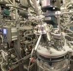
Jim Collins, executive vice president, DuPont, tours the new OLED materials scale-up facility at Stine-Haskell with Avi Avula, global business director, DuPont Displays.
DuPont’s new OLED materials scale-up facility at Stine-Haskell is designed to deliver production scale quantities of advanced materials that enable large-format, solution-based printed OLED displays.
DuPont’s new OLED facility at Stine-Haskell has large-scale formulation systems and can support simultaneous production of multiple product lines.
“Materials are critical to the performance of an OLED TV and we are confident that DuPont has the best performing solution OLED materials available in the market today,” said Avi Avula, global business director, DuPont Displays. “Our vision is that OLEDs will become the display standard and to make that vision a reality, we are focused on helping our customers bring the cost of large sized OLED TVs down to less than $1000 by 2020.”
DuPont’s new scale-up facility is sized to meet the future growth expectations of the OLED TV industry, which analysts predict will increase by over 70 percent for the next several years and will require large quantities of highly sophisticated OLED materials. DuPont has been developing its suite of advanced OLED materials for the last 15 years. These materials are highly regarded for both solution and evaporative applications due to their long lifetime and deep color. In addition to its recently announced collaboration with an inkjet equipment maker to advance solution printed displays, DuPont is actively engaged with the leading OLED display manufacturers to bring solution printed OLED technology to market as quickly as possible.
DuPont’s new OLED facility at Stine-Haskell has large-scale formulation systems and can support simultaneous production of multiple product lines. It was designed with a focus on employee safety, environmental responsibility and producing superior quality materials with the highest possible purity. The project was partially funded by a grant from the state of Delaware in 2012, with DuPont investing more than $20 million in the facility.
DuPont Displays brings more than 15 years of experience in enabling evaporative and solution-based OLED technologies through advanced materials that deliver the color, efficiency and lifetime performance that display manufacturers and consumers demand. DuPont offers highly engineered, next-generation OLED materials as well as solution process know-how that makes the promise of lower cost OLED technology commercially feasible for TVs and other large-format displays.
About DuPont
DuPont has been bringing world-class science and engineering to the global marketplace in the form of innovative products, materials, and services since 1802. The company believes that by collaborating with customers, governments, NGOs, and thought leaders we can help find solutions to such global challenges as providing enough healthy food for people everywhere, decreasing dependence on fossil fuels, and protecting life and the environment.
Share on:


Subscribe
Stay ahead of the technologies shaping the future of electronics with our latest newsletter, Advanced Electronics Packaging Digest. Get expert insights on advanced packaging, materials, and system-level innovation, delivered straight to your inbox.
Subscribe now to stay informed, competitive, and connected.
Suggested Items
AI Demand Drives PCB Material Market Growth
05/08/2026 | TPCAAs AI computing continues to drive a comprehensive upgrade in hardware specifications, the global printed circuit board industry is undergoing a profound structural transformation.
I-Connect007 Editor’s Choice: Five Must-Reads for the Week
05/01/2026 | Michelle Te, I-Connect007If it feels like the PCB industry is accelerating faster than ever, you’re not imagining it. From advanced materials driven by AI applications to renewed investment in domestic manufacturing—and the next generation stepping into critical roles—there’s a lot shifting at once. My selections for this week highlight where the pressure points are forming, and where the opportunities are emerging.
Electronics Manufacturing Needs Your Voice: Global Sentiment Survey Now Live
04/30/2026 | Global Electronics AssociationThe latest monthly Global Sentiment Survey from the Global Electronics Association is now open. At a time when demand uncertainty, policy shifts, energy costs, and supply chain recalibration are pulling the industry in multiple directions, the survey captures something macroeconomic data often misses: how manufacturers are actually experiencing conditions on the ground.
From Backbone to Breakthroughs: I-Connect007 Wraps PCB Materials Series with Focus on Innovation
05/06/2026 | I-Connect007I-Connect007 wraps up its six-part podcast series, PCB Materials: The Backbone and Future of Electronics, with Episode 6 and a discussion focusing on innovation. In Episode 6, Marcy LaRont speaks with Isola CTO Kirk Thompson about a critical turning point for the PCB industry as innovation accelerates. As data rates climb and demands from AI infrastructure, power density, flexible electronics, photonics, and chiplet integration intensify, traditional material assumptions are no longer sufficient.
Jiva Soluboard Getting the Attention It Deserves
04/30/2026 | Marcy LaRont, I-Connect007 MagazineJiva is a newer company that bridges the divide between PCB fabrication and product circularity or sustainability. Jiva Soluboard is the first fully recyclable laminate material ever created for PCB fabrication, and it's not going unnoticed. Stephen Driver, CEO of Jiva, gave us an update at APEX EXPO, including an exciting certification achievement in February.