


 Driving Innovation: Mechanical and Optical Processes During Rigid-flex Production
 It’s Only Common Sense: Your Biggest Competitor Is Complacency
 The Chemical Connection: Onshoring PCB Production—Daunting but Certainly Possible


Orbotech Showcases Its Latest Nuvogo 1000 DI System at APEX
March 15, 2016 | OrbotechEstimated reading time: 1 minute
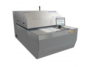
At IPC this week, Orbotech is exhibiting its new Nuvogo 1000 Direct Imaging (DI) system for the PCB manufacturing process. At the show, Orbotech is also presenting, Automated Optical Shaping (AOS) technology.
Orbotech Nuvogo 1000 DI solution brings high accuracy and fast throughput to demanding designs for patterning, solder mask and flex solder mask applications. Utilizing a high-power laser and Orbotech’s unique MultiWave Laser Technology™, the Nuvogo 1000 delivers optimized structures, small undercut and excellent side walls. The high depth-of-focus achieved by field-proven Orbotech Large Scan Optics (LSO) technology ensures unmatched quality on the most challenging surface topographies. The system also offers advanced scaling modes for high precision registration, and a dual table mechanism to optimize imaging time and maximize throughput.
Consistently developing new technologies to improve processes and reduce costs, Orbotech will demonstrate Automated Optical Shaping technology which completes patterns where copper is missing with high precision. This technology, intended to be included in future Orbotech solutions, complements Orbotech’s revolutionary CLS (Closed Loop Shaping) which allows for the accurate removal of excess copper without damaging the laminate.
“The new Nuvogo 1000 DI is another testament to Orbotech’s commitment to bring innovative technologies and cost-effective, high-quality solutions to PCB manufacturers,” said Hadar Himmelman, Orbotech West President. “Furthermore, we believe that our planned AOS technology will soon enable manufacturers to address all defects even in the most advanced PCB designs and to practically eliminate scrap.”
The new Orbotech Nuvogo 1000 system is available now. You can see live demos of the Nuvogo 1000 and learn about Orbotech’s new AOS technology at the IPC APEX EXPO, the premier electronics manufacturing industry event in Las Vegas, NV, Booth #903, March 15-17.
About Orbotech Ltd.
Orbotech Ltd. is a global innovator of enabling technologies used in the manufacture of the world’s most sophisticated consumer and industrial products throughout the electronics and adjacent industries. The Company is a leading provider of yield enhancement and production solutions for electronics reading, writing and connecting, used by manufacturers of printed circuit boards, flat panel displays, advanced packaging, micro-electro-mechanical systems and other electronic components. Virtually every electronic device is produced using Orbotech technology. For more information, click here.
Share on:


Testimonial
"Advertising in PCB007 Magazine has been a great way to showcase our bare board testers to the right audience. The I-Connect007 team makes the process smooth and professional. We’re proud to be featured in such a trusted publication."
Klaus Koziol - atgSuggested Items
BTU International Earns 2025 Step-by-Step Excellence Award for Its Aqua Scrub™ Flux Management System
10/29/2025 | BTU International, Inc.BTU International, Inc., a leading supplier of advanced thermal processing equipment for the electronics manufacturing market, has been recognized with a 2025 Step-by-Step Excellence Award (SbSEA) for its Aqua Scrub™ Flux Management Technology, featured on the company’s Pyramax™ and Aurora™ reflow ovens.
On the Line With… Ultra HDI Podcast—Episode 7: “Solder Mask: Beyond the Traces,” Now Available
10/31/2025 | I-Connect007I-Connect007 is excited to announce the release of the seventh episode of its 12-part podcast series, On the Line With… American Standard Circuits: Ultra HDI. In this episode, “Solder Mask: Beyond the Traces,” host Nolan Johnson sits down with John Johnson, Director of Quality and Advanced Technology at American Standard Circuits, to explore the essential role that solder mask plays in the Ultra HDI (UHDI) manufacturing process.
Rehm Wins Mexico Technology Award for CondensoXLine with Formic Acid
10/17/2025 | Rehm Thermal SystemsModern electronics manufacturing requires technologies with high reliability. By using formic acid in convection, condensation, and contact soldering, Rehm Thermal Systems’ equipment ensures reliable, void-free solder joints — even when using flux-free solder pastes.
Indium Experts to Deliver Technical Presentations at SMTA International
10/14/2025 | Indium CorporationAs one of the leading materials providers to the power electronics assembly industry, Indium Corporation experts will share their technical insight on a wide range of innovative solder solutions at SMTA International (SMTAI), to be held October 19-23 in Rosemont, Illinois.
Knocking Down the Bone Pile: Revamp Your Components with BGA Reballing
10/14/2025 | Nash Bell -- Column: Knocking Down the Bone PileBall grid array (BGA) components evolved from pin grid array (PGA) devices, carrying over many of the same electrical benefits while introducing a more compact and efficient interconnect format. Instead of discrete leads, BGAs rely on solder balls on the underside of the package to connect to the PCB. In some advanced designs, solder balls are on both the PCB and the BGA package. In stacked configurations, such as package-on-package (PoP), these solder balls also interconnect multiple packages, enabling higher functionality in a smaller footprint.