


 It’s Only Common Sense: Marketing Isn’t Fluff, It’s Ammunition
 Driving Innovation: Mechanical and Optical Processes During Rigid-flex Production
 The Chemical Connection: Onshoring PCB Production—Daunting but Certainly Possible


Scientists Study the Insulator-Superconductor Transition of Copper-Oxide Compound in Fine Detail
April 11, 2016 | BNLEstimated reading time: 4 minutes
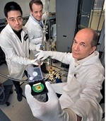
Using a highly controlled deposition technique, scientists from the U.S. Department of Energy's (DOE) Brookhaven National Laboratory have synthesized ultrathin films containing multiple samples of a copper-oxide compound to study the compound's electronic behavior at near absolute zero, or minus 459 degrees Fahrenheit. This technique, as described in a paper published in this week's Online Early Edition of the Proceedings of the National Academy of Sciences, is helping scientists understand how electrons behave as this material transitions from being an insulator to a superconductor capable of carrying electric current with no resistance.
"We are trying to understand the mechanism of the insulator-superconductor transition in a family of compounds called the cuprates. These compounds become superconducting at relatively high temperatures—minus 200 degrees Fahrenheit—in comparison to most superconducting materials, which require temperatures within a few degrees of absolute zero," said Jie Wu, lead author on the paper and a physicist in Brookhaven Lab's Condensed Matter Physics and Materials Science Department. "Characterizing this mechanism may provide insight into how we can make the superconducting temperature even higher, possibly even reaching room temperature."
This capability would enable electricity to be transferred much more efficiently. "Imagine a power line that carries electricity without any energy loss. We could wire the whole planet, resulting in trillions of dollars in savings and reduced environmental impact," said Wu.
Insulator-superconductor transition
In their native state, cuprates are insulators; they do not readily conduct electricity. But cuprates can become superconducting when chemically "doped" with strontium atoms, which produce free-moving electrons that pair up in the crystalline copper-oxide layers where superconductivity is known to occur.
At a certain reduced doping level, however, superconductivity weakens and eventually disappears. As the cuprates' superconducting temperature is lowered to near absolute zero, resistance increases somewhat (a characteristic of insulators) yet conductivity remains quite high (a characteristic of metals). The nature of this strange "insulating" state has been a puzzle to scientists for years.
Solving the puzzle requires a method of fine-tuning the doping level to incrementally approach the quantum critical point—the "tipping" point at which a material is on the cusp of transitioning from one state of electronic order to another, similar to the phase change that happens when ice melts into liquid water. It also requires a highly sensitive way to measure the electronic changes corresponding with the different doping levels.
One film, many samples
To study the insulator-superconductor transition in fine detail, the scientists synthesized films of a compound containing lanthanum, strontium, copper, and oxygen. They used a combinatorial molecular beam epitaxy system at Brookhaven that places materials onto a substrate, atom by atom, in a layered manner and at tightly controlled deposition rates.
Through photolithography, a technique of transferring a geometric pattern onto a substrate, the scientists patterned single-crystal films into a linear "combinatorial" library containing 30 samples, each with a slightly different chemical doping level near the quantum critical point. To provide the electrical contact needed to measure the resistivity of the samples, they evaporated gold pads onto the films' surface.
"We programmed the system to vary the doping level continuously and very precisely at a set minute increment," said Ivan Bozovic, co-author on the paper and a senior physicist in Brookhaven's Condensed Matter Physics and Materials Science Department.
The scientists then measured the electrical resistivity of the samples with varying temperatures, magnetic fields, and doping levels near the quantum critical point. Two types of measurements were taken: one parallel to the electrical current (longitudinal resistivity) and one perpendicular (Hall resistivity).
"The Hall resistivity is much more sensitive because it measures the voltage at a particular cross section of the sample. Longitudinal resistivity averages the whole section," said Wu. "Our Brookhaven team is the first to use this more localized approach that can give us a direct measurement of the density of mobile electrons."
Page 1 of 2
Share on:


Testimonial
"In a year when every marketing dollar mattered, I chose to keep I-Connect007 in our 2025 plan. Their commitment to high-quality, insightful content aligns with Koh Young’s values and helps readers navigate a changing industry. "
Brent Fischthal - Koh YoungSuggested Items
WestDev Announces Advanced Thermal Analysis Integration for Pulsonix PCB Design Suite
10/29/2025 | WestDev Ltd.Pulsonix, the industry-leading PCB design software from WestDev Ltd., announced a major enhancement to its design ecosystem: a direct interface between Pulsonix and ADAM Research's TRM (Thermal Risk Management) analysis software.
Designers Notebook: Power and Ground Distribution Basics
10/29/2025 | Vern Solberg -- Column: Designer's NotebookThe principal objectives to be established during the planning stage are to define the interrelationship between all component elements and confirm that there is sufficient surface area for placement, the space needed to ensure efficient circuit interconnect, and to accommodate adequate power and ground distribution.
Episode 6 of Ultra HDI Podcast Series Explores Copper-filled Microvias in Advanced PCB Design and Fabrication
10/15/2025 | I-Connect007I-Connect007 has released Episode 6 of its acclaimed On the Line with... American Standard Circuits: Ultra High Density Interconnect (UHDI) podcast series. In this episode, “Copper Filling of Vias,” host Nolan Johnson once again welcomes John Johnson, Director of Quality and Advanced Technology at American Standard Circuits, for a deep dive into the pros and cons of copper plating microvias—from both the fabricator’s and designer’s perspectives.
Nolan’s Notes: Tariffs, Technologies, and Optimization
10/01/2025 | Nolan Johnson -- Column: Nolan's NotesLast month, SMT007 Magazine spotlighted India, and boy, did we pick a good time to do so. Tariff and trade news involving India was breaking like a storm surge. The U.S. tariffs shifted India from one of the most favorable trade agreements to the least favorable. Electronics continue to be exempt for the time being, but lest you think that we’re free and clear because we manufacture electronics, steel and aluminum are specifically called out at the 50% tariff levels.
MacDermid Alpha & Graphic PLC Lead UK’s First Horizontal Electroless Copper Installation
09/30/2025 | MacDermid Alpha & Graphic PLCMacDermid Alpha Electronics Solutions, a leading supplier of integrated materials and chemistries to the electronics industry, is proud to support Graphic PLC, a Somacis company, with the installation of the first horizontal electroless copper metallization process in the UK.