


 The Chemical Connection: Onshoring PCB Production—Daunting but Certainly Possible
 Marcy’s Musings: The Legislative Outlook—Helping or Hurting?
 It’s Only Common Sense: The Phone Is Still Mightier Than the Keyboard


AT&S Officially Opens New Plant in China
April 22, 2016 | AT&SEstimated reading time: 5 minutes
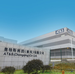
- After Shanghai, another production site opened in China: in the world‘s largest city, Chongqing
- Largest single investment of the AT&S Group, totalling € 480 million; currently 1,700 employees
- Key element in the expansion of technology leadership and further profitable growth of AT&S
- Official opening ceremony with more than 100 guests from politics and business
The site consists of two plants: plant 1 started serial production with one production line in February; plant 2 is currently still being set up. With a total investment volume of roughly € 480 million by 2017, this will be the largest single investment of AT&S to date.
The opening ceremony took place in the presence of representatives of official China and Austria, business, the media, the city of Chongqing, customers, the Supervisory Board and the management of AT&S. The Austrian ambassador in Beijing, Irene Giner-Reichl, Chongqing’s mayor, Huang Qifan, as well as AT&S Supervisory Board Chairman, Hannes Androsch, and CEO Andreas Gerstenmayer held speeches. After the ceremony, selected guests had the opportunity to visit parts of clean room production.
“Chongqing is a key element in the future of AT&S with a view to both technology and positioning, and to further profitable growth. With this plant, we are the first high-end IC substrate manufacturer in China and thus focus on the microelectronics emphasis pursued by the Chinese government at an early stage. Based on the new technologies, combined with the existing high-end technologies, the result is ‘more than AT&S’: we can offer the market new high-end connectivity and advanced packaging solutions and comprehensively position ourselves in the rapidly changing environment of the electronics industry with innovative technologies like IC substrates and wafer level packages for functional modules and the Internet of things. From the PCB top league to the connectivity solution and packaging Champions League, as it were“, says Andreas Gerstenmayer, CEO of AT&S, and adds: “In the medium term, this will entail a new company dimension with revenue of roughly one billion, which will help us to finance future investments from our own cash flow to a greater extent. However, we expect a negative impact during the start-up phase.”
At plant 1, AT&S produces IC substrates, the connection between microchips and printed circuit boards, which are used for microprocessors in computing. Since the start of serial production in late February, the gradual expansion of capacity and the increase in production volume of the complex technology have been proceeding well. From the end of the calendar year 2016, AT&S will gradually start up the second production line for IC substrates. Overall, AT&S will invest roughly € 280 million in property, plant and equipment for this technology by mid-2017.
In addition, the Chongqing site will be extended by a second plant for the latest generation of high-end printed circuit boards, i.e., substrate-like PCBs in order to be able to offer advanced packaging solutions at wafer level. This plant will start production with the first production line in the second half of the calendar year 2016, and with a second production line next year.
Roughly € 200 million will be invested in property, plant and equipment at this plant.
Chen Jian Phua, CEO of the Business Unit Mobile Devices & Substrates, who has been responsible for the establishment of the sites in Shanghai and Chonqing for 12 years for AT&S in leading management positions, outlines the complexity of the technology and the framework conditions: “The new IC substrate technology is not comparable to any technology previously used by AT&S: new, extremely complex production processes in 100 percent cleanroom conditions, new materials as well as a new team, which had to build up know-how in a very short time. We are very proud that we have managed to achieve all this on a very tight schedule. We also invested more than 670,000 hours in training the roughly 1,700 employees who currently work in Chongqing. Sustainable and comprehensive investments in environmental protection have always been important to us at all locations; in Chongqing, about € 24 million have been invested in this area.“
Page 1 of 2
Share on:


Testimonial
"The I-Connect007 team is outstanding—kind, responsive, and a true marketing partner. Their design team created fresh, eye-catching ads, and their editorial support polished our content to let our brand shine. Thank you all! "
Sweeney Ng - CEE PCBSuggested Items
KYZEN Brings Reliability to Life at productronica 2025 with ANALYST² Process Control Demos
10/22/2025 | KYZEN'KYZEN, the global leader in innovative environmentally responsible cleaning chemistries, will exhibit at productronica 2025, November 18–21 in Munich, Germany, where the company will put a spotlight on its award-winning KYZEN ANALYST² process control system in Hall A4, Stand 450.
SCHMID Group Secures Major Orders for AI Server PCB Production Equipment
10/22/2025 | SCHMID GroupSCHMID Group, a global equipment maker and solution provider for Printed Circuit Boards (PCB) and IC-Substrate manufacturing – announced the successful acquisition of two significant orders in the fast-growing field of PCB for artificial intelligence (AI) server applications. So called AI-Server-Boards.
SEMICON Japan 2025 to Spotlight Sustainability in AI and Semiconductor Innovation
10/22/2025 | SEMISEMICON Japan 2025, the largest gathering of leaders from the microelectronics manufacturing supply chain in Japan, will bring together more than 1,200 exhibitors showcasing semiconductor solutions from December 17-19 at Tokyo Big Sight.
Circus SE Set for High-Volume Market Entry in the Defense Sector
10/17/2025 | BUSINESS WIRECircus SE a global technology leader in AI robotics for autonomous nutrition systems and troop supply, is expanding its global production network as part of its high-volume market entry into the defense sector.
China Expands Rare Earth Export Restrictions, Tightening Grip on Global Supply Chains
10/16/2025 | I-Connect007 Editorial TeamChina sharply expanded its rare earth export restrictions on Oct. 9, adding additional elements and refining technologies to its control list while imposing stricter rules on foreign users in the defense and semiconductor industries.