


 Driving Innovation: Mechanical and Optical Processes During Rigid-flex Production
 It’s Only Common Sense: Your Biggest Competitor Is Complacency
 The Chemical Connection: Onshoring PCB Production—Daunting but Certainly Possible


If you want to save on your monthly electric bill and reduce your greenhouse gas emissions at the same time, you might buy a new, energy-efficient refrigerator. Or water heater. Or clothes dryer. But if you can only replace one of these, which will give you the biggest payback?
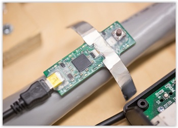
You could try to figure that out by comparing the energy-use labels from your existing appliances with those of the models you might purchase — if you still have your old labels. Even then, the numbers may differ significantly from your actual usage, depending on factors such as age, condition, and your local climate. But soon, there could be a much easier way to figure out exactly how much power is being used by every appliance, lighting fixture, and device in your home, with pinpoint accuracy and at low cost, thanks to devices and software developed by researchers at MIT.
The team’s findings, developed over several years of intensive research, are described in a series of papers, including one published this week in the IEEE Sensors Journal, in a paper by MIT Professor of Electrical Engineering Steven Leeb and recent graduates David Lawrence MEng ’16 and John Donnal PhD ’16. Another paper from the team, which also includes as co-author James Paris PhD ’13, is still in press.
While many groups have worked on developing devices to monitor electricity use, the new MIT system has some key advantages over other approaches. First, it involves no complex installation: No wires need to be disconnected, and the placement of the postage-stamp-sized sensors over the incoming power line does not require any particular precision — the system is designed to be self-calibrating. Second, because it samples data very quickly, the sensors can pick up enough detailed information about spikes and patterns in the voltage and current that the system can, thanks to dedicated software, tell the difference between every different kind of light, motor, and other device in the home and show exactly which ones go on and off, at what times.
Own your own data
Perhaps most significantly, the system is designed so that all of the detailed information stays right inside the user’s own home, eliminating concerns about privacy that potential users may have when considering power-monitoring systems. The detailed analysis, including the potential for specialized analysis based on an individual user’s specific needs or interests, can be provided by customized apps that can be developed using the MIT team’s system.
Tests of the system have showed its potential to save energy and greenhouse emissions — and even to improve safety. One installation at a military base used for training exercises revealed that large tents were being heated all day during winter months, even though they were unoccupied for most of the daytime hours — a significant waste of money and fuel (which, in a combat setting, could be an important logistical concern). Another test installation, in a home, found an anomalous voltage pattern that revealed a wiring flaw that caused some copper plumbing pipes to carry a potentially dangerous live voltage.
“For a long time, the premise has been that if we could get access to better information [about energy use], we would be able to create some significant savings,” Leeb says. He and his students have been tackling the problem for more than 10 years and bit by bit have found ways to circumvent the daunting problems involved in achieving this basic task.
First was the ability to monitor changes in voltage and current without cutting the main incoming power line to a home or business (an expensive process requiring a licensed electrician) or plugging every appliance into a special monitoring device. Other groups have attempted to use wireless sensors to pick up the very faint magnetic and electric fields near a wire, but such systems have required a complex alignment process since the fields in some places can cancel each other out. The MIT team solved the problem by using an array of five sensors, each slightly offset from the others, and a calibration system that tracks the readings from each sensor and figures out which one is positioned to give the strongest signal.
Page 1 of 2
Share on:


Testimonial
"In a year when every marketing dollar mattered, I chose to keep I-Connect007 in our 2025 plan. Their commitment to high-quality, insightful content aligns with Koh Young’s values and helps readers navigate a changing industry. "
Brent Fischthal - Koh YoungSuggested Items
Episode 6 of Ultra HDI Podcast Series Explores Copper-filled Microvias in Advanced PCB Design and Fabrication
10/15/2025 | I-Connect007I-Connect007 has released Episode 6 of its acclaimed On the Line with... American Standard Circuits: Ultra High Density Interconnect (UHDI) podcast series. In this episode, “Copper Filling of Vias,” host Nolan Johnson once again welcomes John Johnson, Director of Quality and Advanced Technology at American Standard Circuits, for a deep dive into the pros and cons of copper plating microvias—from both the fabricator’s and designer’s perspectives.
Nolan’s Notes: Tariffs, Technologies, and Optimization
10/01/2025 | Nolan Johnson -- Column: Nolan's NotesLast month, SMT007 Magazine spotlighted India, and boy, did we pick a good time to do so. Tariff and trade news involving India was breaking like a storm surge. The U.S. tariffs shifted India from one of the most favorable trade agreements to the least favorable. Electronics continue to be exempt for the time being, but lest you think that we’re free and clear because we manufacture electronics, steel and aluminum are specifically called out at the 50% tariff levels.
MacDermid Alpha & Graphic PLC Lead UK’s First Horizontal Electroless Copper Installation
09/30/2025 | MacDermid Alpha & Graphic PLCMacDermid Alpha Electronics Solutions, a leading supplier of integrated materials and chemistries to the electronics industry, is proud to support Graphic PLC, a Somacis company, with the installation of the first horizontal electroless copper metallization process in the UK.
Electrodeposited Copper Foils Market to Grow by $11.7 Billion Over 2025-2032
09/18/2025 | Globe NewswireThe global electrodeposited copper foils market is poised for dynamic growth, driven by the rising adoption in advanced electronics and renewable energy storage solutions.
MacDermid Alpha Showcases Advanced Interconnect Solutions at PCIM Asia 2025
09/18/2025 | MacDermid Alpha Electronics SolutionsMacDermid Alpha Electronic Solutions, a global leader in materials for power electronics and semiconductor assembly, will showcase its latest interconnect innovations in electronic interconnect materials at PCIM Asia 2025, held from September 24 to 26 at the Shanghai New International Expo Centre, Booth N5-E30