


 Marcy’s Musings: Operating Without a Rulebook
 It’s Only Common Sense: Hire for Hunger, Train for Skill
 Dan’s Biz Bookshelf: ‘The 'NVIDIA Way: Jensen Huang and the Making of a Tech Giant’


The Story Behind the News: Ventec’s IMS Manufacturing Capabilities in China Doubled
September 19, 2016 | Pete Starkey, I-Connect007Estimated reading time: 10 minutes
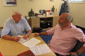
In this interview conducted at Ventec Europe’s headquarters in Leamington Spa, UK, Ventec Europe & USA COO Mark Goodwin sat down with I-Connect007 Technical Editor Pete Starkey to share the details of Ventec International Group’s $2 million equipment investment. With this injection of new equipment, Ventec doubles its IMS material manufacturing capacity in China.
Starkey: Mark, your news release announced that Ventec International Group has invested 2 million dollars, which doubles your capacity to manufacture insulated metal substrate materials in Jiangyin, China. I first saw your IMS manufacturing facility in Suzhou back in 2011, and it was evident then that Ventec had gone to great lengths to address all of the critical factors specific to meeting, and in many cases surpassing, the demands the market was making at that time. What changes have you seen in the last five years?
Goodwin: The first big change was to move on beyond prepreg technology, which was based on our core capability proven over many years of laminate production, using glass fabrics loaded with thermally conductive resin systems, bonded between aluminium as the heat sink and copper as the conductor. The big limitation with that construction is that glass is a very good thermal, as well as electrical insulator, and because our objective is to get the heat out of products, we need thermal conductivity as well as electrical insulation between the heat sink and the conductor. So the major development in technology from what you saw in 2011 to where we are today is that, as well as producing the lower 1.6−2.2-watt thermal performance materials based on woven glass prepreg, we now produce a range of materials, our B-Series, with un-reinforced thermally conductive dielectrics, in the 3.0−10.0-watt range. Taking the glass out significantly improves the thermal conductivity of the insulation layer, and hence you can get heat from the component to the heatsink much more efficiently, particularly useful in high power LED lighting applications.
Starkey: So how has the market demand grown?
Goodwin: Frankly speaking, I don’t have a good handle on the global demand numbers. I know what the demand is for our products—hence we’ve doubled our capacity! Our materials are heading more and more into the automotive lighting space—this is the big driver for us. And the baseline technology for this is a 3-watt material with a dielectric thickness in the range 50 to 100 microns, depending on the customer’s electrical breakdown strength and hi-pot requirements. Obviously the dielectric thickness influences both the electrical and the thermal performance of the material. The thinner the dielectric, the lower the thermal impedance, and vice versa.
Starkey: And would I be right in assuming that in the case of these thin-dielectric materials, when you haven’t got the benefit of the glass fabric to effectively act as a mechanical spacer, you rely very heavily on advances in process engineering and process control to maintain the critical insulation thickness?
Goodwin: That’s been a big driver in the investment we’ve just made. It’s not just been a matter of increasing capacity, we’ve obviously made engineering changes to the equipment to give us tighter control over dielectric thickness, particularly at the 50-micron level. You need better thickness control at this level both to maintain the insulating capabilities of the material—not forgetting that you’ve got the treatment side of the copper foil to fully encapsulate—and to achieve the thermal impedance characteristics the customer requires. This is an ongoing challenge; there are still plans for improvement and we will make further process control enhancements as we continue to run the new equipment. I do know that when we put in the third line we will probably make more engineering changes in line with the ongoing requirements of a developing market.
Starkey: Something that was apparent to me from early on, and I know that your OEM technology team has made a lot of progress in this area, was the challenge of educating the designer in understanding what were the real material characteristics and how to meaningfully define thermal conductivity. In some cases, I believe they were not sure exactly what they were asking for.
Goodwin: I see much less of that today, predominantly because we’re working, not exclusively, but largely, in the automotive lighting sector. The engineering teams at these suppliers of LED lighting, as well as product lines like E-motors and DC power converters, to the automotive business, tend to have a higher level of engineering capability than typical manufacturers of domestic or municipal lighting, which was the business we were talking about five years ago. The guys we’re working with now have a good understanding of materials and a clear vision of what they are trying to achieve. They are pushing us in two directions: thinner dielectrics and higher thermal conductivity. We can make down to 50 microns and up to 10.0 watts per metre kelvin, although the combination of 10.0 watts and 50 microns is probably the practical limit of our technology at the moment and I’m not sure we could deliver it in volume—but we certainly can at 75 microns.
Starkey: What challenges have been encountered and overcome in the IMS manufacturing process to achieve the ultimate in product quality?
Goodwin: The challenges have been two-fold. We have already talked about thickness control in coating. The other challenge is controlling the flow, and hence maintaining thickness control, over the full area of the bonded IMS panel. To produce a sandwich of copper foil, un-reinforced dielectric and aluminium, you’ve obviously got to have some flow. You can’t afford any micro-voids because these would be potential sites for short circuits between aluminium and copper, and you have to maintain hi-pot capability. For example, at the end of our new line everything is edge-linished to remove the copper from the edge of the panel, so that we can do in-line hi-pot testing on every B-series panel produced.
Starkey: Mark, talking about panels, what panel size is typical in manufacture?
Goodwin: The general demand is for sizes like 600 mm x 500 mm or 610 mm x 510 mm. In the B-series, we produce up to 610 mm width and the length in the machine direction is limited only by the size of the press plates, typically 1225 mm. We normally bond the material as two half-sheet panels on full-sheet copper & press plates.
Page 1 of 2
Share on:


Testimonial
"We’re proud to call I-Connect007 a trusted partner. Their innovative approach and industry insight made our podcast collaboration a success by connecting us with the right audience and delivering real results."
Julia McCaffrey - NCAB GroupSuggested Items
Nortech Systems Launches Power over Fiber Technology Platform for EMI-Sensitive Applications
04/08/2026 | Globe NewswireNortech Systems Incorporated, a leading provider of design and manufacturing solutions for complex electromedical devices and electromechanical systems, has announced the launch of its Power over Fiber technology platform.
Flexible Thinking: Designing Flex Circuits for Dynamic Reliability
04/09/2026 | Joe Fjelstad -- Column: Flexible ThinkingFlex circuits flex. No surprises there. However, they are also very commonly designed into products because they are thin and offer consistent thickness and dielectric properties, attributes highly prized by present-day product designers of personal electronics. This would include smartphones and, increasingly, wearable electronics for medical monitoring and even fashion.
Understanding Tolerances in Flexible Circuit Design
04/01/2026 | Chris Clark, Flexible Circuit TechnologiesThe challenge with cumulative tolerances is meeting the dimensional requirements for items dimensioned on a drawing or specification for a flexible or rigid-flex circuit. It is critical to understand the fabrication processes and how features are defined when creating your tolerance requirements.
Target Condition: An Exploration of Flooding PCB Layers
04/02/2026 | Kelly Dack -- Column: Target ConditionThe concept of flooding PCB layers with copper has been around for so long, you’d think we’d have it mastered. We haven’t. (Oh, and by “we,” I mean design engineers and the software tools we depend on.) Years ago, PCB artwork was created by hand using light tables, with tape applied to Mylar. Signals were slow, traces were relatively wide, and high-current paths were simply “beefed up” with wider copper. Signal integrity wasn’t yet a driving concern. Today, solid return paths are fundamental to robust design. We understand the importance of continuous reference planes for signal integrity and EMI control.
New, Greener Solutions for Etch: Novel Copper Extraction
03/30/2026 | Richard Nichols, GreenSource Engineering“Novel” is a typical marketing phrase that implies new and unique, but often “novel” actually means an established technology being applied to a new field or application. This, in turn, is often driven by newly relevant external motivation. GreenSource has been working on just such a solution: novel copper extraction, offering a better and greener alternative to traditional LLE control systems for cupric chloride etch.