


 American Made Advocacy: Smart Policies Can Ensure AI Data Centers Are Secure
 Beyond the Board: Early Engagement Means Faster Prototyping for Defense Programs
 Defense Speak Interpreted: The Autonomous Plane Battle—Skyborg Vs. Loyal Wingman


Researchers Control 'shear-band' Defects in Manufacturing Processes
September 22, 2016 | Purdue UniversityEstimated reading time: 4 minutes
An international team of researchers has invented a method to control the formation of defects called "shear bands" in metals manufacturing processes and discovered microscopic details of how the defects are created.
Shear banding occurs often in high-speed machining of structural metals. It has been a long-standing problem in manufacturing processes because it hinders production of good quality surfaces while machining advanced metal alloys like titanium, nickel and high-temperature aerospace materials, and in the production of metal sheets and foils, according to Srinivasan Chandrasekar, a Purdue University professor of industrial engineering and Kevin P. Trumble, a professor of materials engineering.
"This new work, based on a fundamental understanding of how shear bands form, is an important advance for manufacturing and metals processing," said Chandrasekar, director of Purdue's Center for Materials Processing and Tribology.
The research has revealed that the shear bands form in two phases, said Purdue postdoctoral research associate Koushik Viswanathan.
First, a "weak interface" is created as the metal is being cut, and then the metal shears at this interface, producing a saw-tooth pattern.
The formation of "shear bands" has been a long-standing problem in metals manufacturing processes. The phenomenon is seen in the electron microscope image at left as a wavy saw-toothed structure in a peeled strip of titanium. At right top, the researchers traced a "micromarker" across a shear band, highlighted in yellow. At bottom right an electron back scatter image reveals the band as a severely deformed, dark featureless region about four micrometers thick.
"More importantly, we have learned how to suppress the formation of shear bands using a simple method," said lead author Dinakar Sagapuram, a former Purdue postdoctoral research associate who recently joined Texas A&M University as an assistant professor.
Findings are detailed in a paper published online in August in the Proceedings of the Royal Society A, and featured on the cover of the September print edition of the journal.
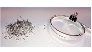
Chandraekar sherbands2 An international team of researchers has invented a method to control the formation of defects called "shear bands" in metals manufacturing processes. At left, the defects create chips of needle-shaped particles. At right, the new method eliminates the shear banding, resulting in a long continuous strip. (Purdue University image/Center for Materials Processing and Tribology) Download image
The phenomenon of shear-band formation exists in many settings, from the nearly atomic scale in "metallic glasses," to the millimeter scale in machined metals and to kilometer-size defects seen in rocks that undergo sliding in the earth's crust.
The "displacement profiles" of shear bands resemble those created in liquids flowing past an interface. Because of this similarity, the researchers applied mathematical equations customarily used to analyze viscous fluid flow to analyze the formation of the shear bands. The fluid-like behavior is mysterious because it is unclear whether the metals being processed heat up enough to actually become liquid.
"The temperatures generated in these shear bands have been estimated from a few hundred Celsius to a few thousand Celsius, so this is really an unknown," Viswanathan said.
The first phase of the band formation occurs within just a few microseconds.
"The second phase is where the metal slides along a thin weak interface," Sagapuram said. "This phase is somewhat more gradual and surprisingly exhibits a viscous-like behavior."
The suppression method works by adding a wedge-shaped die opposite the cutting tool, so that the chip from the metal being machined is channeled between the two. The additional tool constrains the metal to deform more uniformly and eliminates the viscous sliding phase. Because of its simplicity, the method is practical for use in industry.
"You can think of it as the tool consisting of two parts, one doing the cutting and other doing the constraining," said Chandrasekar, also a professor of materials engineering.
The paper was authored by Sagapuram, Viswanathan, Chandrasekar and Trumble; Anirban Mahato, an assistant professor at the Indian Institute of Technology, Patna; Narayan K. Sundaram, an assistant professor at the Indian Institute of Science; and Rachid M'Saoubi, a research manager at Seco Tools Ltd. in the United Kingdom.
The researchers studied the deformation by taking images of marks etched into the metal beforehand. As the metal is processed, the groove-like "micromarkers" reveal the large and serrated deformations.
"The markers basically tell you if the deformation is homogeneous or not, and also how much deformation the material has locally undergone near the shear band defects," Trumble said.
The shear bands form parallel, intensely deformed striations and may cause the metal to break into fragments small enough to produce a powder-like pile of chip shavings. Metals like titanium and magnesium, which have a hexagonal close-packed crystal structure, are particularly prone to the shear band formation. However, the bands can form also in other metals that do not have this crystal structure, including brass, copper, steels and superalloys.
Several patent applications related to the research were filed through the Purdue Research Foundation's Office of Technology Commercialization.
The work was funded by the U.S. Department of Energy, U.S. Army Research Office and National Science Foundation.
Share on:


Testimonial
"We’re proud to call I-Connect007 a trusted partner. Their innovative approach and industry insight made our podcast collaboration a success by connecting us with the right audience and delivering real results."
Julia McCaffrey - NCAB GroupSuggested Items
Trouble in Your Tank: Understanding Interconnect Defects, Part 1
11/04/2025 | Michael Carano -- Column: Trouble in Your TankThis month, I’ll address interconnect defects (ICDs). While this defect continues to rear its ugly head, don’t despair. There are solutions, most of which center on process control and understanding the relationship of the chemistry, materials, and equipment. First, though, let’s discuss ICDs.
WestDev Announces Advanced Thermal Analysis Integration for Pulsonix PCB Design Suite
10/29/2025 | WestDev Ltd.Pulsonix, the industry-leading PCB design software from WestDev Ltd., announced a major enhancement to its design ecosystem: a direct interface between Pulsonix and ADAM Research's TRM (Thermal Risk Management) analysis software.
Designers Notebook: Power and Ground Distribution Basics
10/29/2025 | Vern Solberg -- Column: Designer's NotebookThe principal objectives to be established during the planning stage are to define the interrelationship between all component elements and confirm that there is sufficient surface area for placement, the space needed to ensure efficient circuit interconnect, and to accommodate adequate power and ground distribution.
Episode 6 of Ultra HDI Podcast Series Explores Copper-filled Microvias in Advanced PCB Design and Fabrication
10/15/2025 | I-Connect007I-Connect007 has released Episode 6 of its acclaimed On the Line with... American Standard Circuits: Ultra High Density Interconnect (UHDI) podcast series. In this episode, “Copper Filling of Vias,” host Nolan Johnson once again welcomes John Johnson, Director of Quality and Advanced Technology at American Standard Circuits, for a deep dive into the pros and cons of copper plating microvias—from both the fabricator’s and designer’s perspectives.
Nolan’s Notes: Tariffs, Technologies, and Optimization
10/01/2025 | Nolan Johnson -- Column: Nolan's NotesLast month, SMT007 Magazine spotlighted India, and boy, did we pick a good time to do so. Tariff and trade news involving India was breaking like a storm surge. The U.S. tariffs shifted India from one of the most favorable trade agreements to the least favorable. Electronics continue to be exempt for the time being, but lest you think that we’re free and clear because we manufacture electronics, steel and aluminum are specifically called out at the 50% tariff levels.